Photodetector

A photoelectric detector and photoelectric detection technology, applied in the direction of electric solid-state devices, instruments, circuits, etc., can solve problems such as optical crosstalk

Inactive Publication Date: 2015-04-29
KK TOSHIBA
View PDF5 Cites 9 Cited by
  • Summary
  • Abstract
  • Description
  • Claims
  • Application Information

AI Technical Summary

Problems solved by technology

[0006] In the prior art, however, optical crosstalk between pixels may be caused by multipl

Method used


Image

  • Photodetector
  • Photodetector
  • Photodetector

Examples


example 1

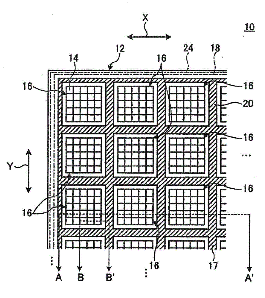
[0084] In the above embodiment, it is described that the antireflection member 20 is continuous and surrounds the pixel regions 16 on the surface of the photodetection layer 12 facing the scintillator layer 18 (see figure 1 )Case. The anti-reflection member 20 only needs to be disposed between the pixels on the surface of the photodetection layer 12 facing the scintillator layer 18, and is not limited to figure 1 Example shown in .

[0085] Figure 13 is a schematic diagram showing a photodetector 10A of the present modified example. Such as Figure 13 As shown in , the antireflection member 20 may be disposed in a discontinuous manner in the direction along the surface between pixels on the surface of the photodetection layer 12 facing the scintillator layer 18 . Except for the arrangement of the anti-reflection member 20 between the pixels, the photodetector 10A is the same as figure 1 The photodetector 10 shown in is the same.

example 2

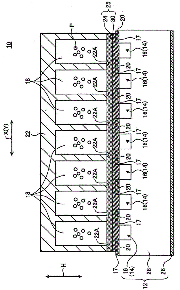
[0087] exist figure 2 In the illustrated example, a case is described in which the antireflection member 20 has a width equal to the distance between pixels. However, the anti-reflection member 20 may have a width smaller than the distance between pixels.

[0088] Figure 14 is a schematic diagram showing a photodetector 10B of the present modified example. Such as Figure 14 As shown, the anti-reflection member 20 may have a distance smaller than the distance between pixels (see Figure 14 The width of W5) in the width (see Figure 14 in the width W4). In addition to the position of the anti-reflection member 20 between pixels is different, the photodetector 10A and figure 2 The photodetector 10 shown is the same.

example 3

[0090] exist figure 2 In the illustrated example, the position and cross-sectional shape of the anti-reflection member 20 in the thickness direction (direction of arrow H) of the photodetector 10 are described so that the anti-reflection member 20 includes light-receiving surfaces corresponding to the APDs 14 position and make the cross-sectional shape protrude from the position to the rectangular shape of the scintillator layer 18 . However, in the thickness direction of the photodetector 10 (see figure 2 The direction of the middle arrow H) the position and cross-sectional shape of the anti-reflection member 20 can be any position and shape so that the anti-reflection member 20 includes areas corresponding to the light-receiving surfaces of the APDs 14, and are not limited to figure 2 Example shown.

[0091] Figure 15 is a schematic diagram showing a photodetector 10C of the present modified example. Such as Figure 15 As shown, in the thickness direction (see Fig...


PUM


Abstract

According to an embodiment, a photodetector includes a scintillator layer (18), a photodetection layer (12), an antireflective member (20), and an intermediate layer (25). The scintillator layer (18) is configured to convert radiation into light. The photodetection layer has a first surface facing the scintillator layer. The photodetection layer includes a pixel region (16) including multiple photodetection devices (14) configured to detect light, and a peripheral region (17) that surrounds the pixel region. The pixel and peripheral regions are provided on the first surface. The antireflective member is provided between the scintillator layer and the photodetection layer and opposed to at least part of the peripheral region. The antireflective member is configured to prevent reflection of at least part of light in a sensitive wavelength range of the photodetection devices. The intermediate layer is provided in a region other than the antireflective member between the scintillator and photodetection layers.

Description

[0001] Cross References to Related Applications [0002] This application is based on, and claims the benefit of priority of, Japanese Patent Application No. 2013-220533 filed on October 23, 2013; the entire contents of which are hereby incorporated by reference. technical field [0003] The invention provides a photodetector. Embodiments described herein relate generally to photodetectors. Background technique [0004] Photodetection devices are known, such as silicon photomultipliers (SiPMs) having a plurality of avalanche photodiodes (APDs) disposed therein. SiPMs are driven in the so-called Geiger mode range by operating the APDs under high reverse bias conditions above the breakdown voltage of these APDs. During operation in Geiger mode, the APD buff is at 10 5 to 10 6 This range is so high that even a photon of faint light can be measured. [0005] Further, a device combining a photodetection device using a plurality of pixels each including a plurality of APDs an...

Claims


Application Information

Patent Timeline
IPC IPC(8): G01T1/20
CPCG01T1/2002H01L27/14663G01T1/20183H01L31/02327H01L31/08
Inventor 佐佐木启太长谷川励
Owner KK TOSHIBA
Why Eureka
Try Eureka