Display baseplate, display panel and display device
A technology for display substrates and alignment marks, which is applied in the fields of display substrates, display panels and display devices, and can solve the problems of exposure equipment alignment and inability to focus, and achieve the effects of excellent preparation quality, high quality, and uniform gray scale
- Summary
- Abstract
- Description
- Claims
- Application Information
AI Technical Summary
Problems solved by technology
Method used
Image
Examples
Embodiment 1
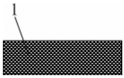
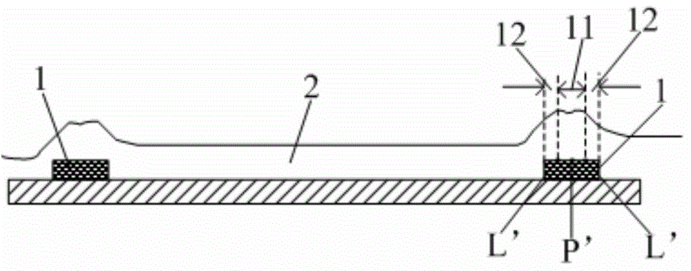
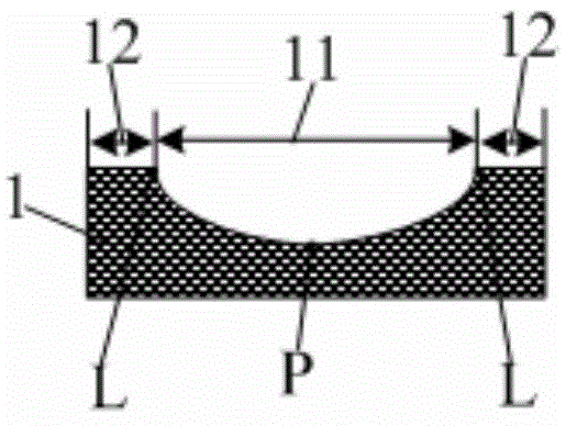
[0029] This embodiment provides a display substrate, such as image 3 and Figure 4 As shown, the alignment mark 1 is included, and the alignment mark 1 is used to align the exposure equipment when exposing and forming the pattern of the first film layer on the display substrate. The thickness of the middle area 11 of the alignment mark 1 is smaller than its edge area 12, so that the thickness of the alignment mark 1 after coating the photoresist 2 is uniform.
[0030] It should be noted that the edge area 12 surrounds the periphery of the middle area 11 . The boundary division between the middle area 11 and the edge area 12 of the alignment mark 1 is divided according to the thickness distribution of the photoresist coated on the alignment mark 1 with a flat surface in the prior art, that is, the corresponding photoresist 2 The area with a thicker distribution is defined as the middle area 11, and the area with a thinner distribution of the photoresist 2 corresponding to th...
Embodiment 2
[0038] This embodiment provides a display substrate, which is different from Embodiment 1 in that Figure 5As shown, the thickness of the middle area 11 of the alignment mark 1 is uniform, and the thickness of the edge area 12 of the alignment mark 1 is uniform.
[0039] Since the alignment mark 1 on the display substrate is usually designed very small (this is mainly to make the alignment mark 1 not occupy too much area on the display substrate), the middle area 11 and the edge area of the alignment mark 1 The area of 12 is correspondingly very small, and the above arrangement of the alignment mark 1 can fully realize the uniform thickness of the alignment mark 1 after being coated with photoresist. Therefore in the present embodiment, the above-mentioned setting of alignment mark 1 can also make the surface after alignment mark 1 is coated with photoresist completely flat, so that the surface gray scale of alignment mark 1 after coating photoresist is uniform, and the li...
Embodiment 3
[0042] This embodiment provides a display substrate, which is different from Embodiment 1-2 in that the display substrate is an array substrate, and the alignment marks are made of metal materials or insulating materials. The first film layer includes a pixel electrode layer, a gate metal layer, a source-drain metal layer, an active layer or a common electrode layer.
[0043] In this embodiment, the metal material used in the alignment mark can be the metal material used in any one of the pixel electrode layer, gate metal layer, source-drain metal layer or common electrode layer. Of course, the alignment mark can also use material that forms the active layer. In addition, the alignment mark can also be made of the same material as that of any insulating layer (such as a gate insulating layer or a passivation layer) in the array substrate. With such an arrangement, the alignment mark and a certain film layer on the array substrate can be prepared and formed at the same time th...
PUM
 Abstract
Description
Claims
Application Information


