Pixel structure and organic light emitting display adopting same

A pixel structure, pixel technology, applied in semiconductor devices, electric solid devices, electrical components, etc., can solve the problems of graininess and streaks, increased aperture width, poor display effect, etc., to improve graininess and streaks. , increase the width, and display the effect of fine

Active Publication Date: 2015-04-29
KUNSHAN GO VISIONOX OPTO ELECTRONICS CO LTD
View PDF7 Cites 21 Cited by
  • Summary
  • Abstract
  • Description
  • Claims
  • Application Information

AI Technical Summary

Problems solved by technology

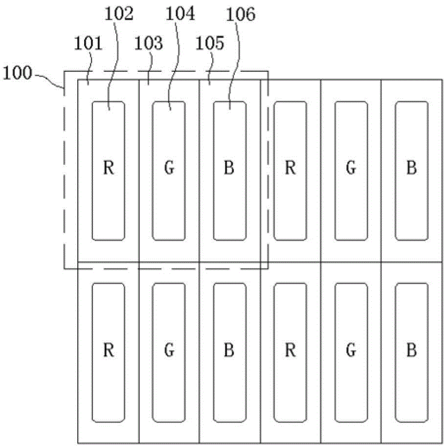
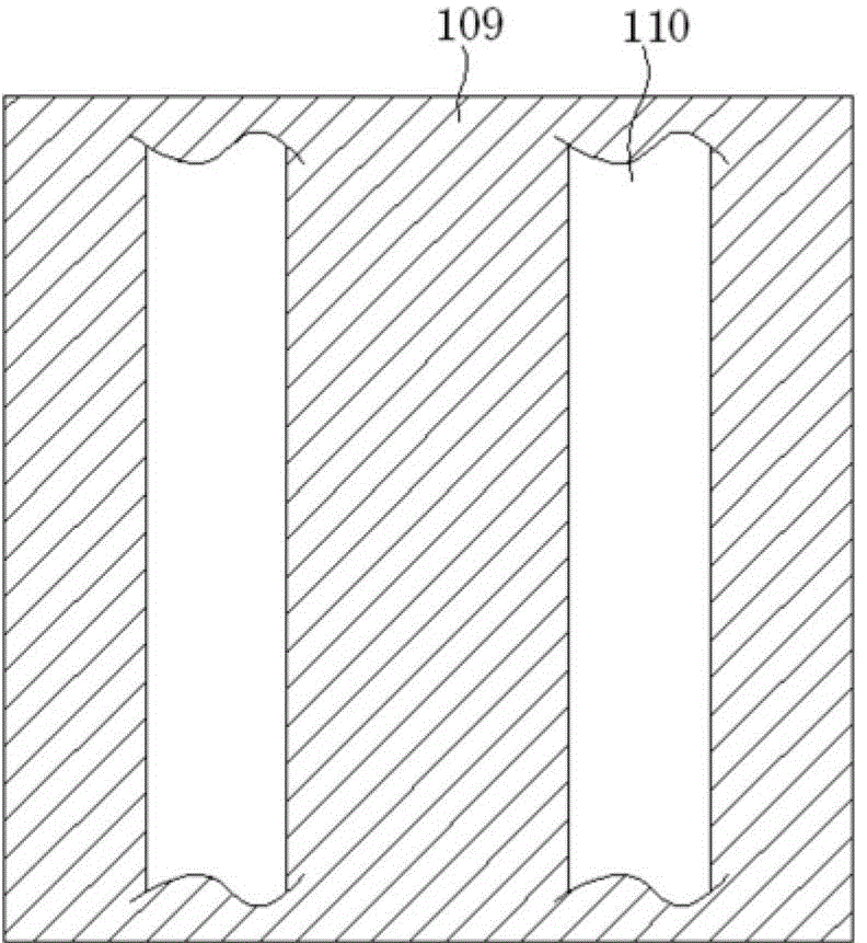
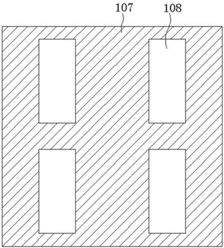
The adjacent pixel units are arranged in a mirror image, so that the 4 R sub-pixels and 4 G sub-pixels are put together separately, and can be evaporated in the Slot method, and the B sub-pixels are arranged in a line, and can be evaporated in the Slit method. , such an arrangement structure can increase the aperture width of the evaporat

Method used


Image

  • Pixel structure and organic light emitting display adopting same
  • Pixel structure and organic light emitting display adopting same
  • Pixel structure and organic light emitting display adopting same

Examples


Example Embodiment

[0031] The present invention will be further described below with reference to the accompanying drawings and specific embodiments, so that those skilled in the art can better understand and implement the present invention, but the examples cited are not intended to limit the present invention.

[0032] Such as Figure 4 As shown, the pixel structure of the present invention includes a plurality of pixel units 400. Each pixel unit 400 is composed of upper and lower halves forming a rhombus. The pixel units 400 in adjacent rows are arranged alternately; each pixel unit 400 It includes a plurality of areas. The first area constitutes one of the upper and lower halves of the diamond-shaped pixel unit 400, and the second area and the third area are arranged side by side to form the other of the upper and lower halves of the diamond-shaped pixel unit 400. Each pixel unit 400 includes multiple sub-pixels, the multiple sub-pixels of the pixel unit 400 are correspondingly distributed in mu...


PUM


Abstract

The invention discloses a pixel structure and an organic light emitting display adopting the same. The pixel structure comprises a plurality of pixel units, wherein each pixel unit takes a rhombus structure formed by an upper half part and a lower half part; the adjacent pixel units are arranged in a staggered manner; each pixel unit comprises a plurality of sub pixels; a first sub pixel forms one of the upper half part and the lower half part of the rhombus pixel unit; a second sub pixel and a third sub pixel are arranged side by side to form the other of the upper half part and the lower half part of the rhombus pixel unit together; pixels in the same color of the pixel units in the adjacent rows are arranged adjacently. By integrating the same sub pixels together, the width of the corresponding vapor deposition Mask hole diameter can be enlarged, the difficulty of the Mask technology can be reduced, and the display PPI (Pixel Per Inch) can be improved; meanwhile, because of the staggered arrangement manner of the pixel units in the adjacent rows, the adjacent edges of the second sub pixel and the third sub pixel with the first sub pixel can be longer, main light emitting of the pixel units can be relatively concentrated, and the light mixing effect is good.

Description

technical field [0001] The present invention relates to the field of organic light-emitting display technology, in particular to a pixel structure and an organic light-emitting display using the pixel structure. Background technique [0002] OLED (Organic Light-Emitting Diode, organic light-emitting diode) is an active light-emitting device. Compared with the traditional LCD (Liquid Crystal Display, liquid crystal display) display method, OLED display technology does not require a backlight and has the characteristic of self-luminescence. OLEDs use very thin layers of organic materials and glass substrates that emit light when an electric current passes through them. Therefore, OLED displays can significantly save power, can be made lighter and thinner, can withstand a wider range of temperature changes than LCD displays, and have a larger viewing angle. OLED display is expected to become the next-generation flat panel display technology after LCD, and it is one of the mos...

Claims


Application Information

Patent Timeline
IPC IPC(8): H01L27/32
Inventor 刘将汪俊
Owner KUNSHAN GO VISIONOX OPTO ELECTRONICS CO LTD
Why Eureka
Try Eureka