Array substrate, manufacturing method thereof, and display device

A technology of an array substrate and a manufacturing method, which is applied in the display field, can solve the problems of increased charge asymmetry, increased signal delay and afterimage, large leakage current, etc., and achieves the effects of reducing power consumption, reducing parasitic capacitance, and reducing overlapping capacitance.

Active Publication Date: 2017-08-29
BOE TECH GRP CO LTD
View PDF3 Cites 0 Cited by
  • Summary
  • Abstract
  • Description
  • Claims
  • Application Information

AI Technical Summary

Problems solved by technology

[0003] However, the low-temperature polysilicon semiconductor material itself has a large leakage current, which increases the degree of charge asymmetry when the display panel performs positive and negative frame inversion, which eventually leads to afterimage phenomenon
In addition, the signal delay of the gate line and the parasitic capacitance of the thin film transistor area will aggravate the afterimage phenomenon

Method used


Image

  • Array substrate, manufacturing method thereof, and display device
  • Array substrate, manufacturing method thereof, and display device
  • Array substrate, manufacturing method thereof, and display device

Examples


Embodiment Construction

[0042] Specific embodiments of the present invention will be described in detail below in conjunction with the accompanying drawings. It should be understood that the specific embodiments described here are only used to illustrate and explain the present invention, and are not intended to limit the present invention.

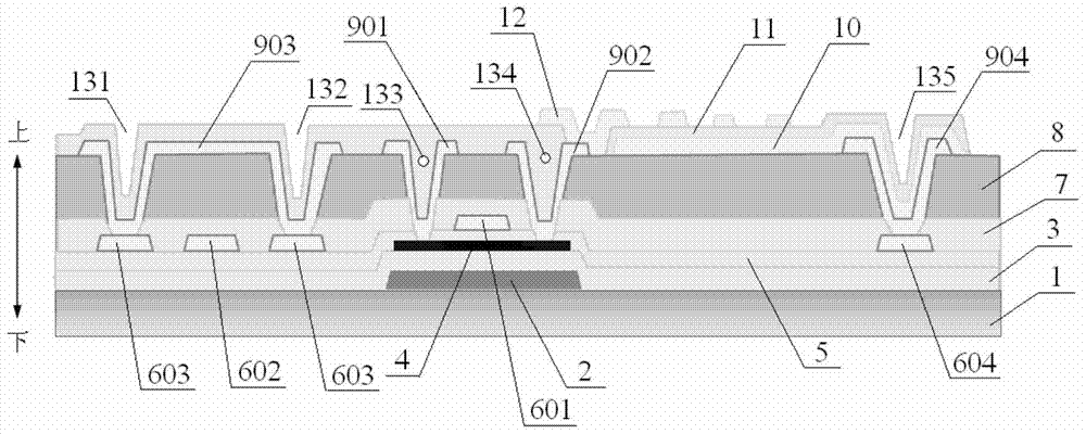
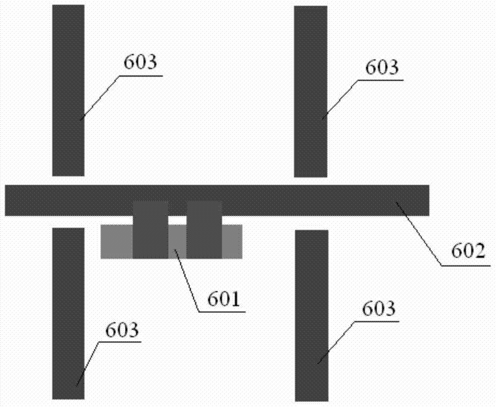
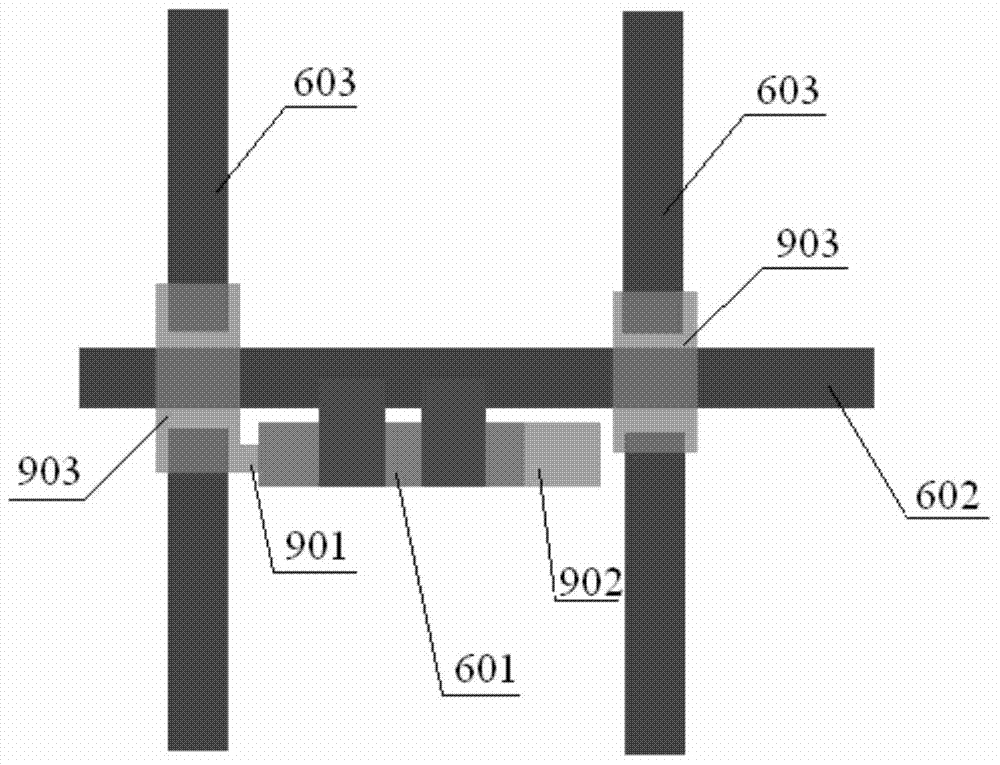
[0043] The present invention firstly provides an array substrate, such as Figure 1-Figure 3 As shown, the array substrate includes a first pattern layer and a second pattern layer sequentially arranged above the base substrate 1 , and an organic insulating layer is arranged between the first pattern layer and the second pattern layer. Wherein, the first pattern layer (refer to figure 2 ) includes a gate 601 of the thin film transistor, a gate line 602, and a data line 603, the gate 601 is connected to the gate line 602, the data line 603 is disconnected by the gate line 602, and the data line 603 is insulated from the gate line 602. The second pattern layer ...


PUM


Abstract

The invention discloses an array substrate, a manufacturing method of the array substrate and a display device. The array substrate comprises a first pattern layer and a second pattern layer which are sequentially arranged on a substrate base plate. An organic insulating layer is arranged between the first pattern layer and the second pattern layer. The first pattern layer comprises a grid electrode of a thin film transistor, a grid line and data lines, wherein the grid electrode is connected with the grid line, the data lines are cut off through the grid line, and the data lines and the grid line are insulated and separated. The second pattern layer comprises a source electrode of the thin film transistor, a drain electrode of the thin film transistor and connection portions, wherein the source electrode is connected with the data lines, the data lines correspond to the connection portions respectively, and each connection portion is used for connecting the portions, located on the two sides of the grid line, of the corresponding data line. By means of the array substrate, the manufacturing method and the display device, the parasitic capacitance of the source electrode, the drain electrode and the grid electrode can be reduced, the overlap capacitance of the grid line and the data lines can be recued, and therefore the signal delay is reduced, the power consumption is lowered, and the residual image phenomenon can be eliminated.

Description

technical field [0001] The present invention relates to the field of display technology, in particular to an array substrate and a manufacturing method thereof, and a display device including the array substrate. Background technique [0002] Low-temperature polysilicon (LTPS) materials are widely used in high-performance liquid crystal display devices (LCD) and light-emitting diode display devices (AMOLED) due to their extremely high mobility. Moreover, the array substrate based on low-temperature polysilicon material can integrate the driving circuit on the glass substrate, which is beneficial to realize narrow frame design and low power consumption display. [0003] However, the low-temperature polysilicon semiconductor material itself has a large leakage current, which increases the degree of charge asymmetry when the display panel performs positive and negative frame inversion, and finally leads to afterimage phenomenon. In addition, the signal delay of the gate line a...

Claims


Application Information

Patent Timeline
Patent Type & Authority Patents(China)
IPC IPC(8): H01L21/77H01L27/12
CPCH01L27/124H01L27/1259
Inventor 舒适孙双徐传祥齐永莲牛菁
Owner BOE TECH GRP CO LTD
Why Eureka
Try Eureka