


Quick Research
Generate reliable direction feasibility study reports for your R&D in just a few steps.

Technical Q&A
Discover and master advanced knowledge NOW. Basics, ideas, possibilities, all at once.

Find Solutions
As an expert in R&D theories, this can generate solutions to your technical problems instantly.

Evaluate Feasibility
Analyze your overall solution with one click, know your potential R&D risks in advance.

Monitor Landscape
Get weekly tech updates, stay abreast of the latest tech innovations and key insights.
Lead frame and chip package thereof
A chip packaging and lead frame technology, which is applied to semiconductor devices, semiconductor/solid-state device components, electric solid-state devices, etc., to achieve the effects of simple and low process, simple structure and low cost
- Summary
- Abstract
- Description
- Claims
- Application Information
AI Technical Summary
Problems solved by technology
Method used
Image

Examples
Embodiment 1
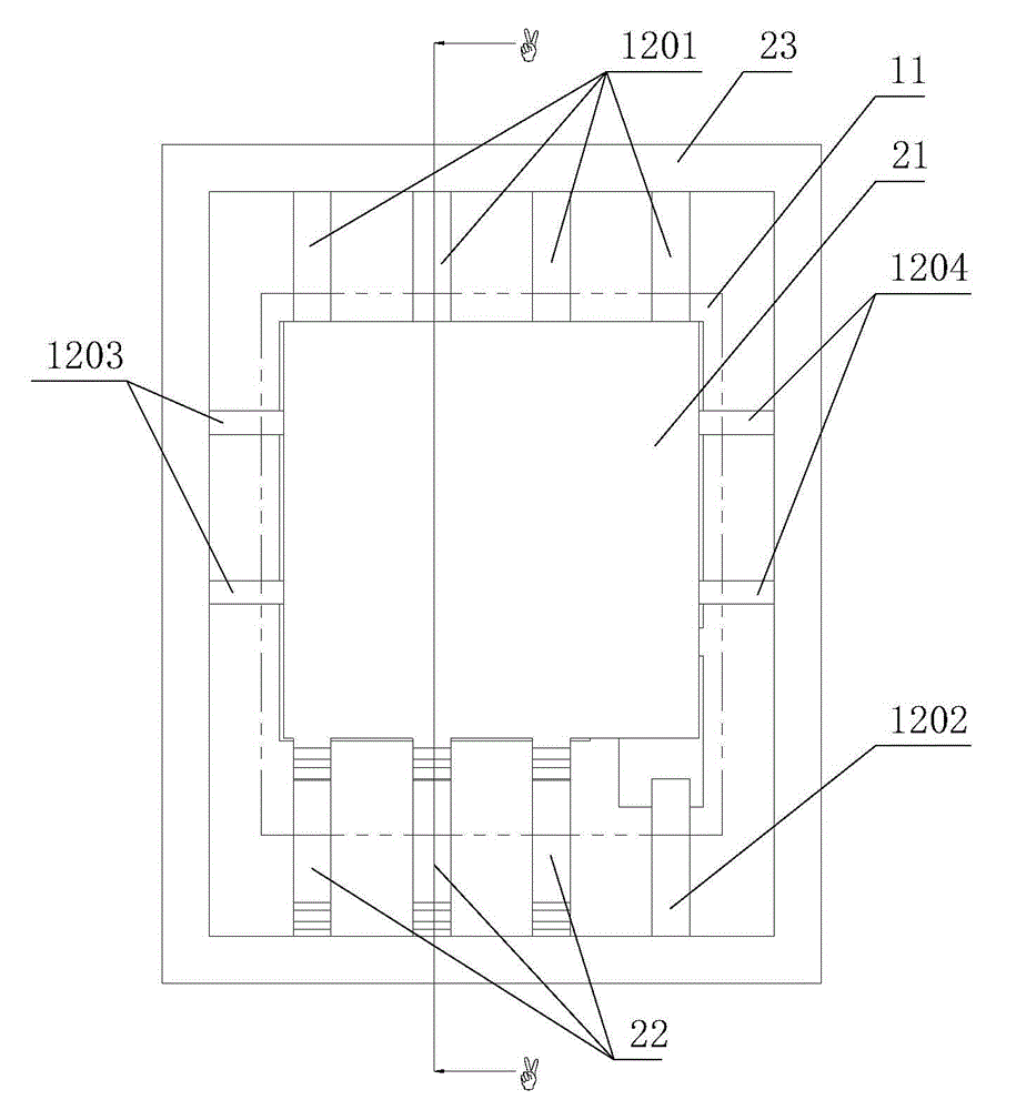
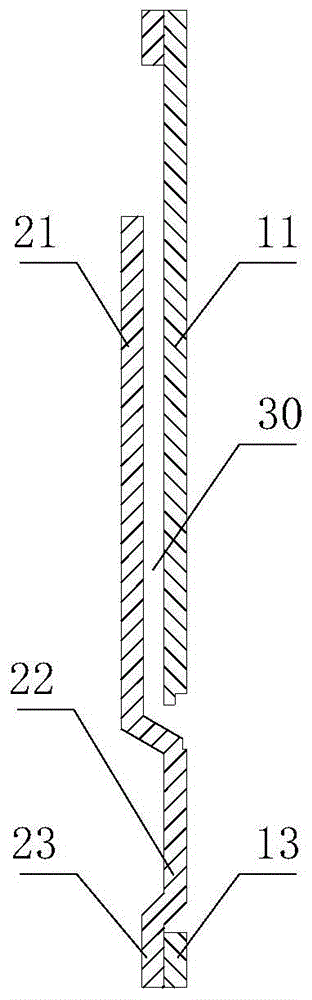
[0057] refer to Figure 1 to Figure 4 , a lead frame provided in Embodiment 1 of the present invention includes a first lead frame 10 and a bridge frame 20,
[0058] The first lead frame 10 includes a first chip holder 11, a plurality of first external pins 12 and a first frame 13, the outer ends of the first external pins 12 are connected to the first frame 13, Its inner end is connected to the first chip holder 11, and the first external pin 12 is provided on the top, bottom, left and right of the first chip holder 11, which are 1201, 1202, 1203, 1204 in sequence, so There is a gap 14 between the first external pins 1203 and 1202,
[0059]The bridge frame 20 includes a second chip holder 21, a plurality of second external pins 22 and a second outer frame 23, the outer ends of the second outer pins 22 are connected to the second outer frame 23, and the inner The end is connected with the second chip holder 21, the second external pin 22 is bent into a groove shape, and the ...
Embodiment 2
[0065] The chip package provided in this embodiment is packaged by the lead frame provided in the first embodiment.
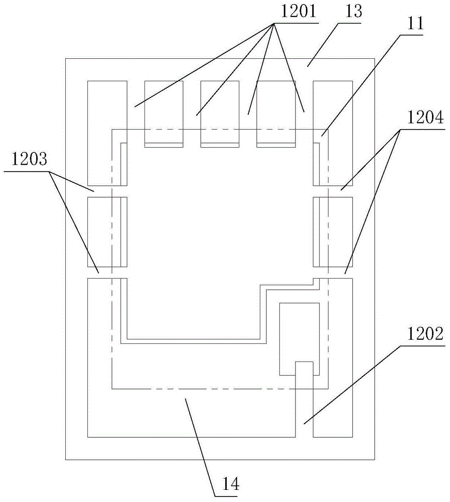
[0066] refer to Figure 5 to Figure 8 , a chip package provided in Embodiment 2 of the present invention, comprising:
[0067] The first lead frame 10, the first lead frame 10 includes a first chip holder 11, a plurality of first external pins 12, the inner ends of the first external pins 12 are connected to the first chip holder 11, The first chip holder 11 is provided with first external pins 12 on the top, bottom, left, and right, which are composed of 1201, 1202, 1203, and 1204 in sequence, and the first external pins 1203 and 1202 are arranged between There are vacancies14;
[0068] A bridge frame 20, the bridge frame 20 is stacked on the first lead frame 10, the bridge frame 20 includes a second chip holder 21, a plurality of second external pins 22, and the second external pins 22 The inner end of the pin is connected to the second chip holder 21, the...
Embodiment 3
[0075] The chip package provided in this embodiment is packaged by the lead frame provided in the first embodiment.
[0076] refer to Figure 9 to Figure 12 The main difference between the chip package provided by Embodiment 3 of the present invention and the chip package provided by Embodiment 2 is that the upper surface of the bridge frame 20 leaks outside the encapsulant 50, and this difference is further improved. Heat dissipation of the chip package. Other structures are the same as those in Embodiment 2.
PUM
 Abstract
Description
Claims
Application Information
 - R&D Engineer
- R&D Manager
- IP Professional
- Industry Leading Data Capabilities
- Powerful AI technology
- Patent DNA Extraction
Browse by: Latest US Patents, China's latest patents, Technical Efficacy Thesaurus, Application Domain, Technology Topic, Popular Technical Reports.
© 2024 PatSnap. All rights reserved.Legal|Privacy policy|Modern Slavery Act Transparency Statement|Sitemap|About US| Contact US: help@patsnap.com