Solar control coated glass capable of being used in one piece and preparation method of solar control coated glass
A solar control and coated glass technology, applied in the direction of coating, etc., can solve the problems of poor acid and alkali resistance and salt spray corrosion resistance, inability to provide mechanical protection for the functional layer, and poor scratch resistance of the surface protective layer, etc., to achieve Salt spray corrosion resistance, high temperature oxidation resistance, excellent scratch resistance performance, excellent decorative effect
- Summary
- Abstract
- Description
- Claims
- Application Information
AI Technical Summary
Problems solved by technology
Method used
Image
Examples
Embodiment 1
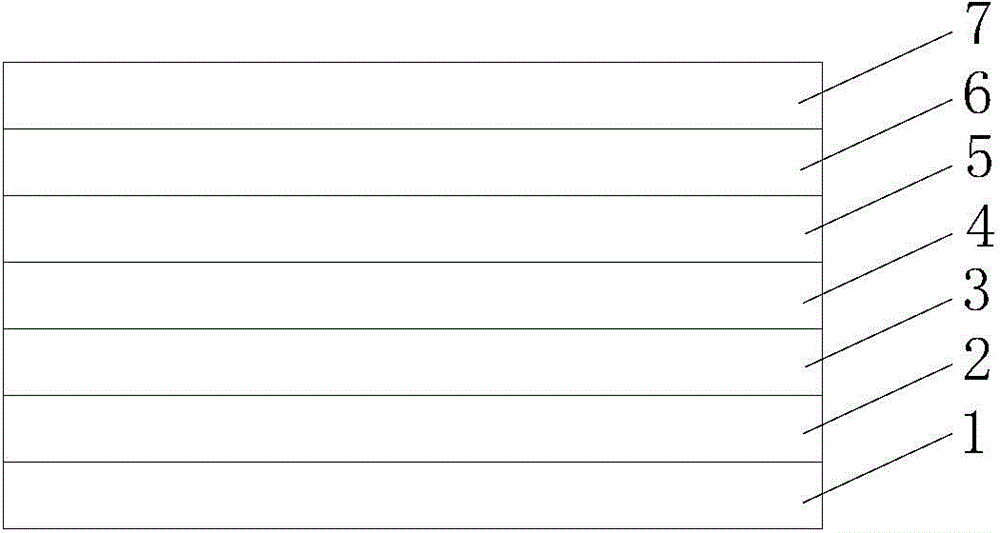
[0028] figure 1 It is a schematic diagram of the layer structure of the coated glass according to the embodiment of the present invention. refer to figure 1 , the solar control coated glass that can be used in a single piece in this embodiment includes a solar control film layer plated from the glass substrate 1 and one side of the glass substrate 1 in sequence. The outward order is the dielectric barrier layer 2 , the first sacrificial layer 3 , the functional layer 4 , the second sacrificial layer 5 , the dielectric support layer 6 and the top protective layer 7 . In this embodiment, the glass substrate 1 is ordinary float glass with a thickness of 6 mm; the dielectric barrier layer 2 is Si 3 N 4The film layer has a thickness of 42nm; the first sacrificial layer 3 is a NbZr film layer with a thickness of 2nm; the functional layer 4 is a NiCr film layer with a thickness of 6nm; the second sacrificial layer 5 is a NbZr film layer with a thickness of 2nm; dielectric support ...
Embodiment 2
[0041] According to the optical constant of the single-layer film and the principle of thin film interference, in this example, a coated glass with a glass surface reflection color different from that of Example 1 was prepared. This embodiment differs from Embodiment 1 only in that the dielectric barrier layer 2 is Si 3 N 4 The film layer has a thickness of 30nm; the first sacrificial layer 3 is a NbZr film layer with a thickness of 2nm; the functional layer 4 is a NiCr film layer with a thickness of 4nm; the second sacrificial layer 5 is a NbZr film layer with a thickness of 2nm; dielectric support layer 6 is Si 3 N 4 Film layer, the thickness is 28nm; the top protective layer 7 is ZrYO X film with a thickness of 13 nm.
[0042] In the embodiment of the present invention, the thickness of the glass substrate 1 can be any thickness, such as the common specifications of existing glass, such as 3mm, 5mm, 6mm, 8mm, 12mm, etc. The function of the dielectric barrier layer 2 dir...
PUM
| Property | Measurement | Unit |
|---|---|---|
| thickness | aaaaa | aaaaa |
| thickness | aaaaa | aaaaa |
| thickness | aaaaa | aaaaa |
Abstract
Description
Claims
Application Information
 - R&D
- Intellectual Property
- Life Sciences
- Materials
- Tech Scout
- Unparalleled Data Quality
- Higher Quality Content
- 60% Fewer Hallucinations
Browse by: Latest US Patents, China's latest patents, Technical Efficacy Thesaurus, Application Domain, Technology Topic, Popular Technical Reports.
© 2025 PatSnap. All rights reserved.Legal|Privacy policy|Modern Slavery Act Transparency Statement|Sitemap|About US| Contact US: help@patsnap.com


