Fluorescence imaging device and method

A fluorescence imaging and fluorescence technology, applied in the field of optical imaging, can solve the problems of slow image acquisition speed, difficult installation and debugging, low light source utilization rate, etc., achieve higher speed, improve stability and reliability, and simplify complex structures Effect

Inactive Publication Date: 2015-05-13
BEIJING HAIWEIER TECH DEV
View PDF10 Cites 6 Cited by
  • Summary
  • Abstract
  • Description
  • Claims
  • Application Information

AI Technical Summary

Problems solved by technology

[0004] The technical problem to be solved by the present invention is to provide a fluorescent imaging device and method, which solves the problem of complex structure, difficult installation and debugging, slow image acquisition speed, high cost, low light source utilization rate and heat dissipation of the traditional large-area non-scanning fluorescent imaging system. Defects such as poor characteristics

Method used


Image

  • Fluorescence imaging device and method
  • Fluorescence imaging device and method
  • Fluorescence imaging device and method

Examples


Embodiment 1

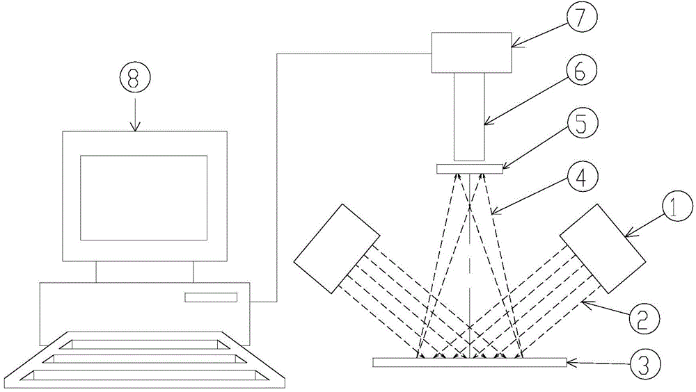
[0022] Embodiment 1. A fluorescent imaging device, which will be combined below figure 1 A detailed description of a fluorescent imaging device provided in this embodiment

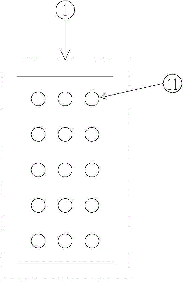
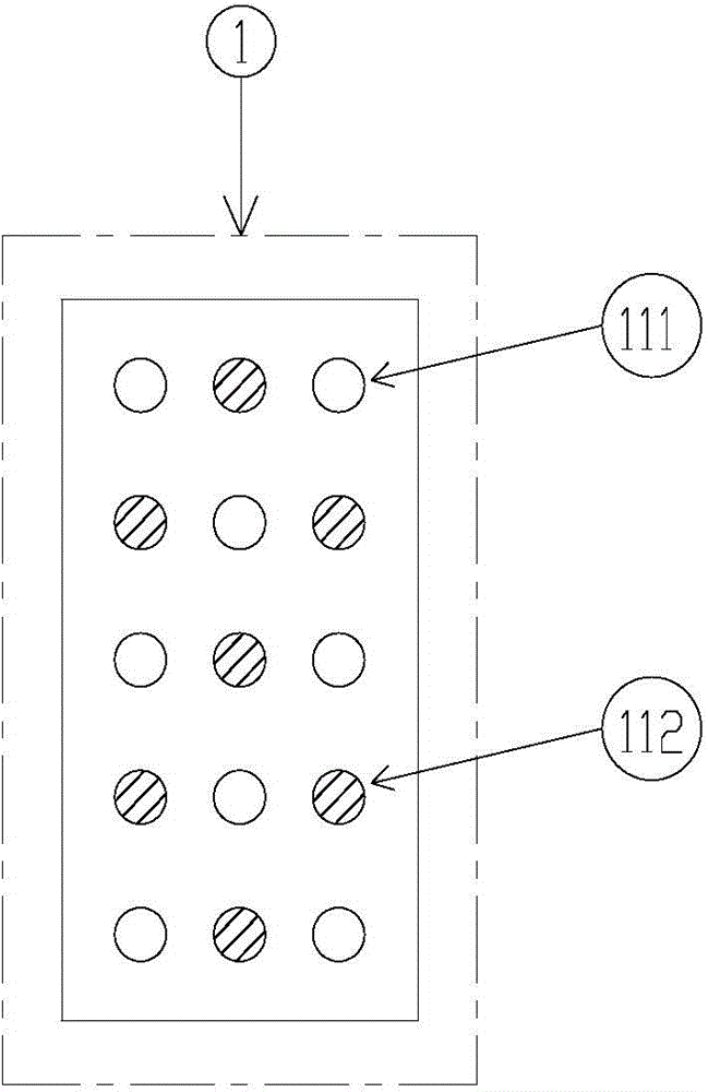
[0023] Such as figure 1 As shown, a schematic diagram of the structure of a fluorescence imaging device, including at least one set of laser light source 1, a sample to be tested 3, an optical filter 5, an imaging lens 6, an image sensor 7 and an intelligent terminal 8. The optical filter 5 is located above the sample 3 and facing the lower port of the imaging lens 6 , the image sensor 7 is fixed on the upper end of the imaging lens 6 , and the image sensor 7 is connected to a smart terminal 8 . The figure shows two groups of laser light sources 1, the laser light source 1 emits excitation light 2 and irradiates the sample 3 to be tested to generate fluorescence 4, the fluorescence 4 irradiates on the optical filter 5, and the fluorescence 4 Only the fluorescence of a specific wavelength passes through t...

Embodiment 2

[0031] Embodiment 2. A fluorescent imaging method. A fluorescent imaging method provided in this embodiment will be described in detail below.

[0032] A fluorescence imaging method comprising:

[0033] Laser light source 1 emits excitation light 2 to irradiate the sample to be tested 3 and generate fluorescence 4;

[0034] The fluorescent light 4 is irradiated onto the optical filter 5, and only the fluorescent light of a specific wavelength in the fluorescent light 4 passes through the optical filter 5 and is irradiated into the imaging lens 6;

[0035] The imaging lens 6 collects fluorescence of a specific wavelength and focuses it on the image sensor 7;

[0036] The image sensor 7 converts the fluorescent optical signal into an electrical signal, and at the same time collects two-dimensional spatial position information to form spatial image information and send it to the intelligent terminal 8;

[0037] The smart terminal 8 displays spatial images.

[0038] A plurality o...


PUM


Abstract

The invention relates to a fluorescence imaging device and method. The device comprises at least one group of laser sources, a to-be-tested sample, an optical color filter, an imaging lens, an image sensor and an intelligent terminal. An optical filter is positioned above the to-be-tested sample and fixedly arranged on the lower end of the imaging lens, the image sensor is fixedly arranged on the upper end of the imaging lens and connected with the intelligent terminal; the laser sources emit laser to be irradiated onto the to-be-tested sample and generate fluorescence which is irradiated onto the optical color filter, only fluorescence with specific wavelength in the fluorescence can penetrate through the optical color filter and irradiate into the imaging lens, and is focused on the image sensor by the imaging lens. According to the fluorescence imaging device, the image acquiring speed and the irradiation uniformity of the laser excited light can be improved, the stability and reliability of equipment can be improved, the cost can be effectively lowered, the utilization rate of the light source can be increased, and the heat radiation characteristic can be greatly improved.

Description

technical field [0001] The invention relates to the field of optical imaging, in particular to a fluorescence imaging device and method. Background technique [0002] Due to the single-spectrum characteristics of the laser, the light of the appropriate wavelength emitted by the laser light source is the most ideal excitation light source for fluorescence detection. However, due to the high orientation of the laser light source itself and the inability to uniformly illuminate large-area samples, the current application of laser light sources in the field of fluorescence detection is limited to single-point detection or linear detection. Since single-point detection or linear detection can only detect one point or one line at a time, current detection systems of this type must use highly complex motion mechanisms to obtain two-dimensional fluorescence images of the sample to be tested. Therefore, due to the existence of the moving structure, the overall structure of this type...

Claims


Application Information

Patent Timeline
Patent Type & Authority Applications(China)
IPC IPC(8): G01N21/64G01N21/01
Inventor 张哲夫
Owner BEIJING HAIWEIER TECH DEV
Why Eureka
Try Eureka