Method for eliminating filter inductor noise caused by chopper
A technology of filter inductors and choppers, which is applied in the field of power supply processing and adjustment, and can solve problems such as destroying comfort
- Summary
- Abstract
- Description
- Claims
- Application Information
AI Technical Summary
Problems solved by technology
Method used
Image
Examples
Embodiment 1
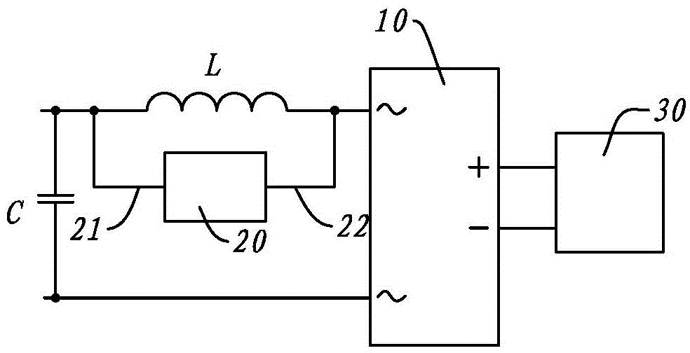
[0025] like figure 1 and figure 2 Shown is a schematic diagram of Embodiment 1 of the present invention. figure 1 It is a schematic diagram of the structure of the electrical appliance where it is located. figure 2 is the structure of the splitter 20 .
[0026] This embodiment is applied to electrical appliances with a power frequency series filter inductor L; C is a filter capacitor, and its two ends are connected to the power signal input obtained by chopping; the rear stage of the filter inductor L is a rectifier bridge 10, and the rear stage of the rectifier bridge Level is load 30. A shunt device 20 is connected in parallel at both ends of the filter inductance L; the output terminals 21 and 22 of the shunt device 20 are mutually conducted when the operating voltage of the filter inductance L in series reaches or exceeds a preset limit peak value; in the filter inductance L When its operating voltage is lower than the limit peak value, it will resume cut-off.
[00...
Embodiment 2
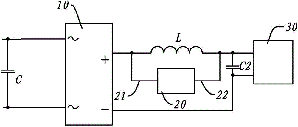
[0032] like image 3 and Figure 4 Shown is a schematic diagram of Embodiment 2 of the present invention. image 3 is the circuit structure of its electrical appliances, Figure 4 It is the structure of the branching part of the present embodiment.
[0033] In this embodiment, the filter inductor L is located at the rear stage of the rectifier bridge 10 , and besides C, the filter capacitor also has C2 at the rear stage. The shunt component 20 is still connected to both ends of the filter inductor L through the output terminals 21 and 22 . It can be seen that the position of the filter inductor L does not affect the effect of the scheme.
[0034] The shunt device 20 of this solution also works in a passive manner. The difference is that this embodiment adopts the form of a shunt unit, and the voltage regulator tube D3 is used in the shunt unit to drive the three-terminal control device—the thyristor T1 to work, so as to reduce excessive voltage. peak. The regulator tube ...
Embodiment 3
[0036] like Figure 5 As shown, the structure diagram of the flow splitting device 20 in this implementation is smooth. The scheme of this embodiment is the same as Figure 4 The structure of the first embodiment shown, this scheme also uses the form of a shunt unit, and each shunt unit uses a three-terminal control device and a voltage regulator tube. The difference is that the shunt unit of this embodiment is located before the rectifier bridge 10, so it is located in the AC In the loop, it is necessary as Figure 5 The structure of two anti-parallel flow splitters in . The three-terminal control devices of this scheme are transistors T3 and T4, which are controlled by regulator tubes D5 and D6 respectively. This solution cuts the voltage spike to achieve a faster response speed.
PUM
 Abstract
Description
Claims
Application Information
 - R&D
- Intellectual Property
- Life Sciences
- Materials
- Tech Scout
- Unparalleled Data Quality
- Higher Quality Content
- 60% Fewer Hallucinations
Browse by: Latest US Patents, China's latest patents, Technical Efficacy Thesaurus, Application Domain, Technology Topic, Popular Technical Reports.
© 2025 PatSnap. All rights reserved.Legal|Privacy policy|Modern Slavery Act Transparency Statement|Sitemap|About US| Contact US: help@patsnap.com


