Supercharge Your Innovation With Domain-Expert AI Agents!

QFN (quad flat nolead) IC (integrated circuit) packaging body and design method thereof

A quadrilateral flat, integrated circuit technology, applied in the direction of circuits, electrical solid devices, electrical components, etc., can solve the problems of reducing the flexibility of trace routing and via layout

Active Publication Date: 2015-05-20
BELL SEMICON LLC
View PDF3 Cites 0 Cited by
  • Summary
  • Abstract
  • Description
  • Claims
  • Application Information

AI Technical Summary

Problems solved by technology

This can be a problem as it reduces flexibility regarding trace routing and via placement, especially where the size of the PWB or PCB is small, such as when used in cellular phones or PDAs

Method used


Image

  • QFN (quad flat nolead) IC (integrated circuit) packaging body and design method thereof
  • QFN (quad flat nolead) IC (integrated circuit) packaging body and design method thereof
  • QFN (quad flat nolead) IC (integrated circuit) packaging body and design method thereof

Examples


Embodiment Construction

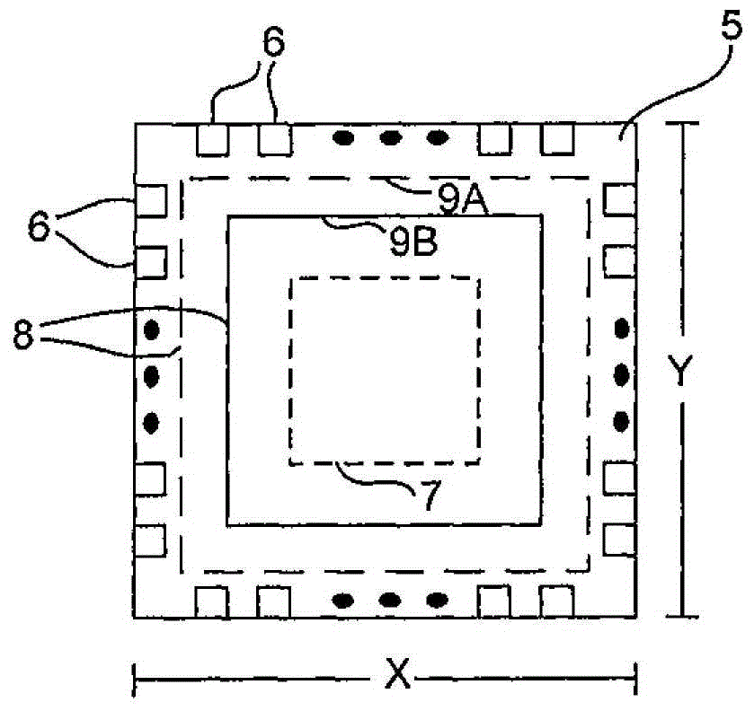
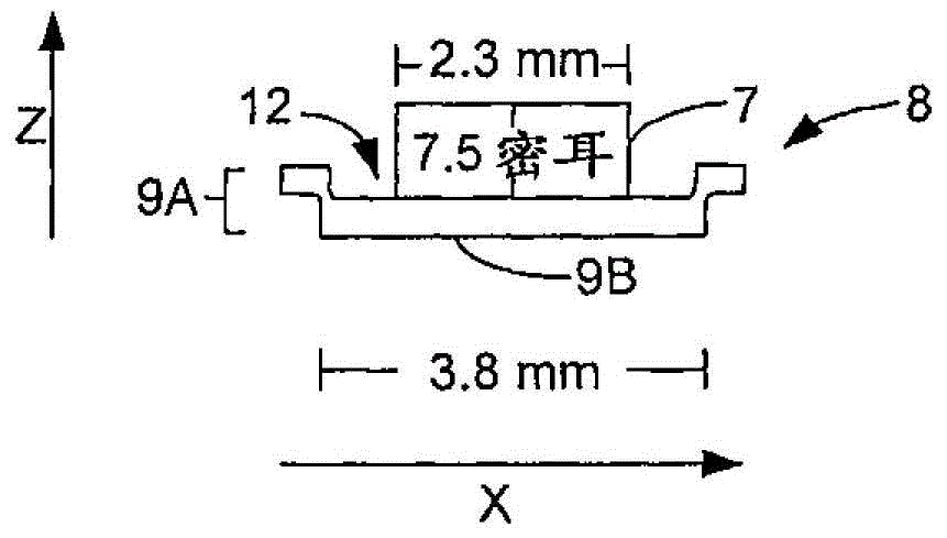
[0020] In accordance with the present invention, there is provided a QFN IC package that has all the advantages of the typical QFN IC package described above, in addition, is configured to facilitate traceability on a PWB or PCB on which the IC package is mounted. Solder pads for routing and / or via placement. By configuring the pads as needed or desired to facilitate routing and / or via placement, the overall size of the PWB or PCB can be reduced without sacrificing the thermal or electrical performance advantages provided by the pads. In addition, reduction in the overall size of the PWB or PCB leads to cost reduction. Some examples of the ways in which pads may be configured to meet these objectives will now be described with reference to some exemplary embodiments. The present invention is not limited to these examples. These embodiments are described to illustrate the principles and concepts of the invention.

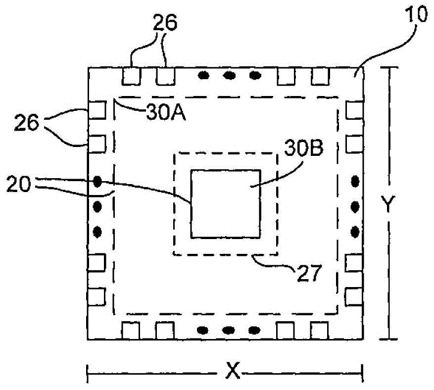
[0021] image 3 Shown is a bottom plan view of a QFN IC pack...


PUM


Abstract

The invention relates to a QFN (quad flat nolead) IC (integrated circuit) packaging body with an improved welding pad and a design method of the packaging body. The QFN IC packaging body has the characteristics that all advantages of the typical QFN IC packaging body are realized; the packaging body is provided with the welding pad for trace wiring and / or hole penetrating arrangement on a PWB (printed wiring board) or a PCB (printed circuit board) which is provided with the IC packaging body; the welding pad is arranged according to the requirements or expectations, so as to facilitate the wiring and / or hole through arrangement; under the condition of not sacrificing the heat or electric property advantage provided by the welding pad, the overall dimension of the PWB or the PCB is reduced; as the overall dimension of the PWB or the PCB is reduced, the cost is reduced.

Description

[0001] Divisional application information [0002] The patent application of the present invention is that the application date is February 12, 2007, the application number is 200780052230.0, and the title of the invention is "quad flat no-lead (QFN) integrated circuit (IC) package with improved pads and for designing the A divisional application of the invention patent application for the method of encapsulation. technical field [0003] The present invention relates to integrated circuits (ICs), and more particularly to quad flat no-leads (QFN) ICs having paddles modified to facilitate printed wiring on which the QFN IC is mounted Routing and / or via placement in the printed circuit board (PWB) or printed circuit board (PCB). Background technique [0004] The original QFN ICs were designed by Amkor Technologies of Chandler, Arizona, but other companies also manufacture and sell QFN IC packages, such as Texas Instruments of Dallas, Texas. A typical QFN IC package includes ...

Claims


Application Information

Patent Timeline
Patent Type & Authority Applications(China)
IPC IPC(8): H01L23/31H01L23/495H01L21/60
Inventor L·W·高里克S·E·海内斯T·J·皮尔雅
Owner BELL SEMICON LLC
Features
  • R&D
  • Intellectual Property
  • Life Sciences
  • Materials
  • Tech Scout
  • Unparalleled Data Quality
  • Higher Quality Content
  • 60% Fewer Hallucinations
Learn More