Pixel demarcation layer and OLED (organic light emitting diode) device

A pixel-defining layer and pixel technology, which is applied in the manufacture of electric solid-state devices, semiconductor devices, and semiconductor/solid-state devices, etc., can solve the problems of easy ink overflow, cross color, and small aperture ratio of red pixel units.

Active Publication Date: 2015-05-20
BOE TECH GRP CO LTD
View PDF5 Cites 22 Cited by
  • Summary
  • Abstract
  • Description
  • Claims
  • Application Information

AI Technical Summary

Problems solved by technology

[0005] However, due to the longer wavelength of red light, the optical cavity length of its pixel is also longer, so the film thickness of the light-emitting layer of the red light material is relatively thick; on this basis, for the OLED device using the above design, in When organic light-emitting materials are produced by solution methods such as inkjet printing methods, since the red pixel unit has a small aperture ratio, its ink holding capacity is relatively small, and its film thickness is relatively thick, so it requires more ink
Based on the above reasons, it will cause the ink in the red pixel unit to easily overflow into other adjacent pixel units, resulting in cross-color

Method used


Image

  • Pixel demarcation layer and OLED (organic light emitting diode) device
  • Pixel demarcation layer and OLED (organic light emitting diode) device
  • Pixel demarcation layer and OLED (organic light emitting diode) device

Examples


Embodiment Construction

[0028] The following will clearly and completely describe the technical solutions in the embodiments of the present invention with reference to the accompanying drawings in the embodiments of the present invention. Obviously, the described embodiments are only some, not all, embodiments of the present invention. Based on the embodiments of the present invention, all other embodiments obtained by persons of ordinary skill in the art without making creative efforts belong to the protection scope of the present invention.

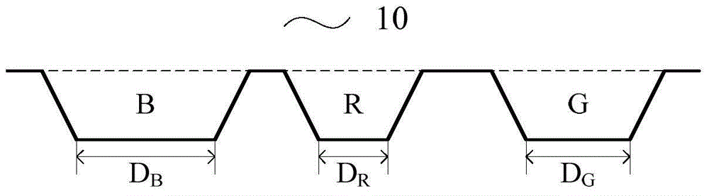
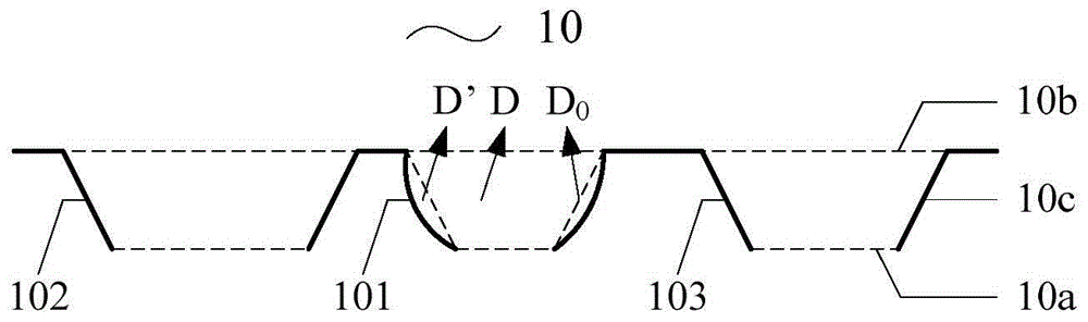
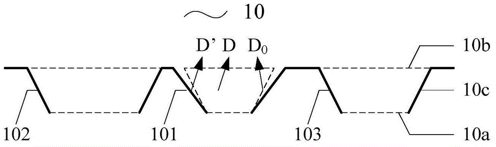
[0029] Embodiments of the present invention provide a pixel defining layer 10, such as Figure 2 to Figure 4 As shown, it includes a plurality of openings for defining pixel units of different colors, and the openings have a bottom opening 10a, a top opening 10b, and a side wall 10c between them.

[0030] The pixel unit at least includes a first pixel unit and a second pixel unit, and the opening at least includes a first opening 101 for defining the first pix...


PUM


Abstract

The embodiment of the invention provides a pixel demarcation layer and an OLED (organic light emitting diode) device, and relates to the technical field of display. The attenuation state of luminous materials of each pixel unit can be identical, and in addition, the color staining caused by solution overflow can be avoided. The pixel demarcation layer comprises a plurality of openings, wherein each opening comprises a bottom surface opening, a top surface opening and a side wall, the openings at least comprise a first opening for limiting a first pixel unit and a second opening for limiting a second pixel unit, the first opening is filled with first pixel luminous materials, the second opening is filled with second pixel luminous materials, the attenuation speed of the first pixel luminous materials is lower than the attenuation speed of the second pixel luminous materials, the bottom surface opening area of the first opening is smaller than the bottom surface opening area of the second opening, the side wall of each opening is provided with a preset reference surface, the space limited by each opening comprises a main body space in the reference surface and an expansion space outside the reference surface; the expansion space size of the first opening is greater than the expansion space size of the second opening. The pixel demarcation layer is used for preparing the OLED device.

Description

technical field [0001] The invention relates to the field of display technology, in particular to a pixel defining layer and an OLED device. Background technique [0002] OLED (Organic Light Emitting Diode, Organic Light Emitting Diode) display devices have attracted extensive attention due to their characteristics such as self-illumination, wide viewing angle, fast response, and flexibility. [0003] At present, in OLED devices, the properties of different color light-emitting materials are quite different; among them, the performance of red-light materials is better, the performance of green-light materials is second, and the performance of blue-light materials is the worst. In this way, during the use of the OLED device, the attenuation speed of the red light material is relatively slow, while the attenuation speed of the blue light material is relatively fast, which will lead to a serious color shift problem. [0004] In order to ensure that the attenuation state of eac...

Claims


Application Information

Patent Timeline
Patent Type & Authority Applications(China)
IPC IPC(8): H01L51/50H01L51/54
CPCH10K59/35H10K59/122H10K50/11H10K59/30
Inventor 崔颖胡春静
Owner BOE TECH GRP CO LTD
Why Eureka
Try Eureka