
Array substrate and manufacturing method thereof, display panel and testing method thereof, and display device

A technology for array substrates and display panels, which is applied in semiconductor/solid-state device testing/measurement, optics, instruments, etc. It can solve problems such as bad materials, waste, and lead wire damage, and achieve cost reduction, lead open-circuit test avoidance, and process simplification. Effect

Active Publication Date: 2015-05-27
BOE TECH GRP CO LTD +1
View PDF5 Cites 25 Cited by
  • Summary
  • Abstract
  • Description
  • Claims
  • Application Information

AI Technical Summary

Problems solved by technology

However, due to the limitation of the design space of some products, the signal line of the short-circuit bar circuit cannot pass through the area where the above-mentioned leads are located and the fan-out area (Fan-out) of the liquid crystal panel, resulting in Even if there is an open circuit and a short circuit in the connecting line, the test mode cannot be detected by switching the switch.
[0004] Therefore, for the COG panel in the above situation, the full contact (Full Contact) method will cause a large number of probe misalignment phenomena because the probe spacing is not small enough (Pin Miss, that is, a part of the lead or terminal in the test area does not touch the probe. ), it will also damage the lead wires, resulting in defects and waste of materials; while the above-mentioned Shorting Bar (Shorting Bar) switch conversion test method cannot detect the open circuit of the lead wires generated in a part of the area, and the test effect cannot be achieved.
Based on the above reasons, none of the existing conventional test methods can realize the lead open circuit test of this type of COG panel

Method used


Image

  • Array substrate and manufacturing method thereof, display panel and testing method thereof, and display device
  • Array substrate and manufacturing method thereof, display panel and testing method thereof, and display device
  • Array substrate and manufacturing method thereof, display panel and testing method thereof, and display device

Examples


Embodiment Construction

[0042] In order to make the purpose, technical solutions and advantages of the embodiments of the present invention clearer, the technical solutions in the embodiments of the present invention will be clearly and completely described below in conjunction with the drawings in the embodiments of the present invention. Obviously, the described embodiments It is a part of embodiments of the present invention, but not all embodiments. Based on the embodiments of the present invention, all other embodiments obtained by persons of ordinary skill in the art without creative efforts fall within the protection scope of the present invention.

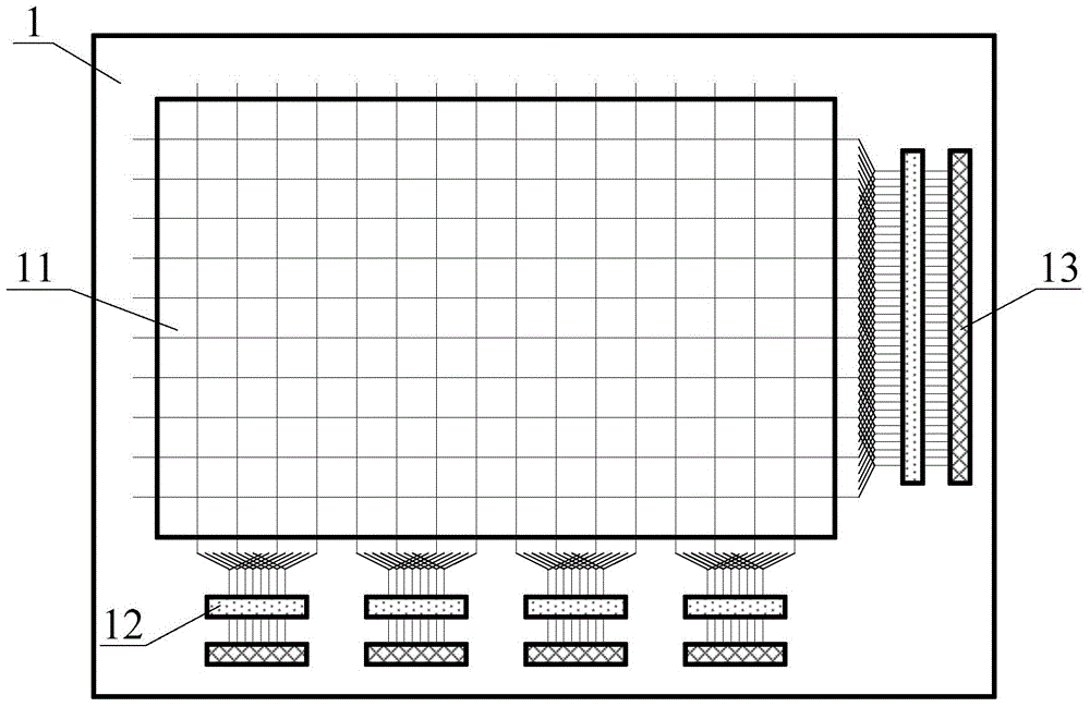
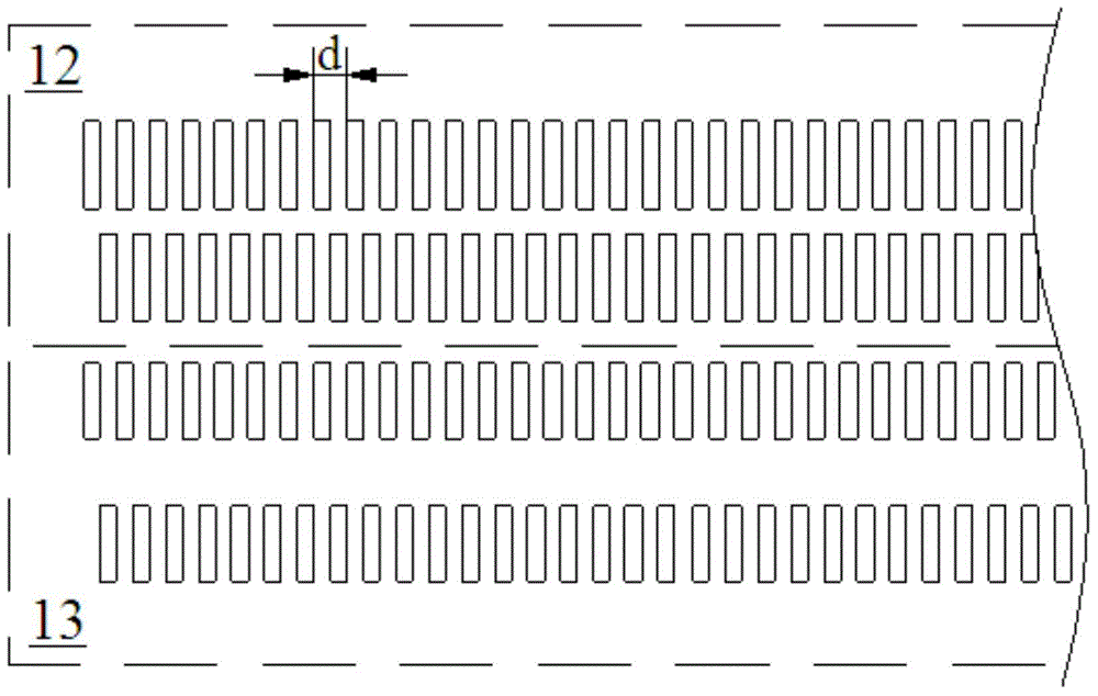
[0043] figure 1 It is a top view structure diagram of an array substrate in an embodiment of the present invention. see figure 1 , the array substrate 1 includes a display area 11 and at least one binding area 12 ( figure 1 Only five binding areas are used as an example), and at least one binding area 12 is located outside the display area 11. ...


PUM


Abstract

The invention provides an array substrate and a manufacturing method thereof, a display panel and a testing method thereof, and a display device. The array substrate comprises a display area and at least one binding area, wherein the at least one binding area is located outside the display area; multiple signal lines are arranged in the display area, and multiple terminals connected with the multiple signal lines by multiple first leads are arranged in the binding area; the array substrate also comprises one or more testing areas corresponding to any one or more of the binding areas; and multiple testing ends are arranged in each testing area, and the multiple testing ends in any one testing area are connected with the multiple terminals in the corresponding binding area by multiple second leads. Compared with a traditional testing mode that a display panel cannot carry out lead open-circuit test, according to the invention, the lead open-circuit test can be implemented.

Description

technical field [0001] The present invention relates to the field of display technology, in particular to an array substrate and a manufacturing method, a display panel and a testing method thereof, and a display device. Background technique [0002] In the existing COG (Chip On Glass, chip on glass) liquid crystal panel, since the driving chip needs to be bound in the bonding area on the glass substrate, the lead spacing between the chip and the substrate is getting smaller and smaller. The trend (for example, around 15 μm). Therefore, if the open circuit (Open) test is to be performed on this part of the leads according to the conventional full contact (Full Contact) method, the probe spacing of the test probe set must also reach the same level. However, the minimum pitch between the probes of the existing probe set is only about 30 μm, so it is impossible to realize the lead open circuit test through the full contact method. Moreover, any test method that uses the conne...

Claims


Application Information

Patent Timeline
IPC IPC(8): G02F1/13G02F1/1333H01L27/12
CPCG02F1/1309H01L27/1214G02F1/13452G02F1/13458H01L22/34H01L22/32H01L27/1259H01L27/124
Inventor 郑尧燮边征朱金伟
Owner BOE TECH GRP CO LTD
Learn More