Level shifting circuit and method for GOA-framework liquid crystal panel

A level shift circuit and level shift technology, applied in instruments, static indicators, etc., can solve the problems of affecting the cost of IC, the size of PCBA, and the cost of PCBA, so as to reduce the total number of traces and pins. number, the effect of reducing the package size

Active Publication Date: 2015-06-03
TCL CHINA STAR OPTOELECTRONICS TECH CO LTD
View PDF4 Cites 33 Cited by
  • Summary
  • Abstract
  • Description
  • Claims
  • Application Information

AI Technical Summary

Problems solved by technology

[0007] Although the above-mentioned level shift circuit for the GOA structure liquid crystal panel can increase the voltage of each control signal to drive the TFT in the liquid crystal panel, when more and more timing signals CKVn are required, the timing controller 100 and There will be more and more pins needed between the level shifting chips 200, and each extra pin may make the package type (package) of the timing controller 100 and the level shifting chip 200 larger, The size of the package model directly affects the cost of the IC
At the same time, more traces will also increase the size of the PCBA, which will further increase the cost
Therefore, when the number of timing signals CKVn required is large, the cost of IC and PCBA will increase significantly, which is not conducive to the original intention of reducing costs by using the GOA architecture.

Method used


Image

  • Level shifting circuit and method for GOA-framework liquid crystal panel
  • Level shifting circuit and method for GOA-framework liquid crystal panel
  • Level shifting circuit and method for GOA-framework liquid crystal panel

Examples


Embodiment Construction

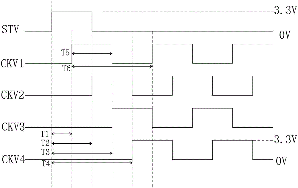
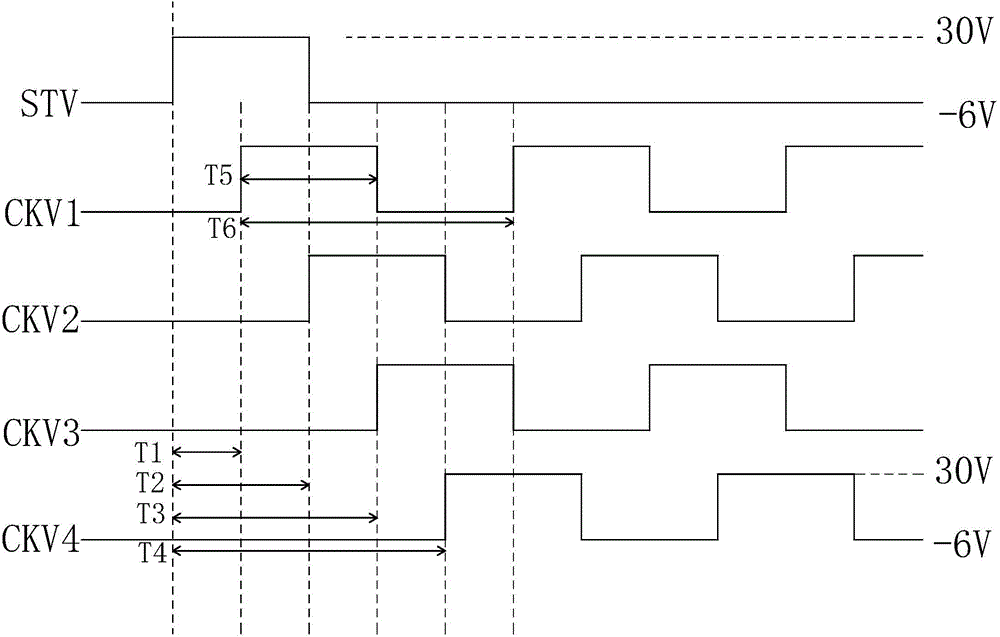
[0039] In order to further illustrate the technical means and effects adopted by the present invention, the following describes in detail in conjunction with preferred embodiments of the present invention and accompanying drawings.

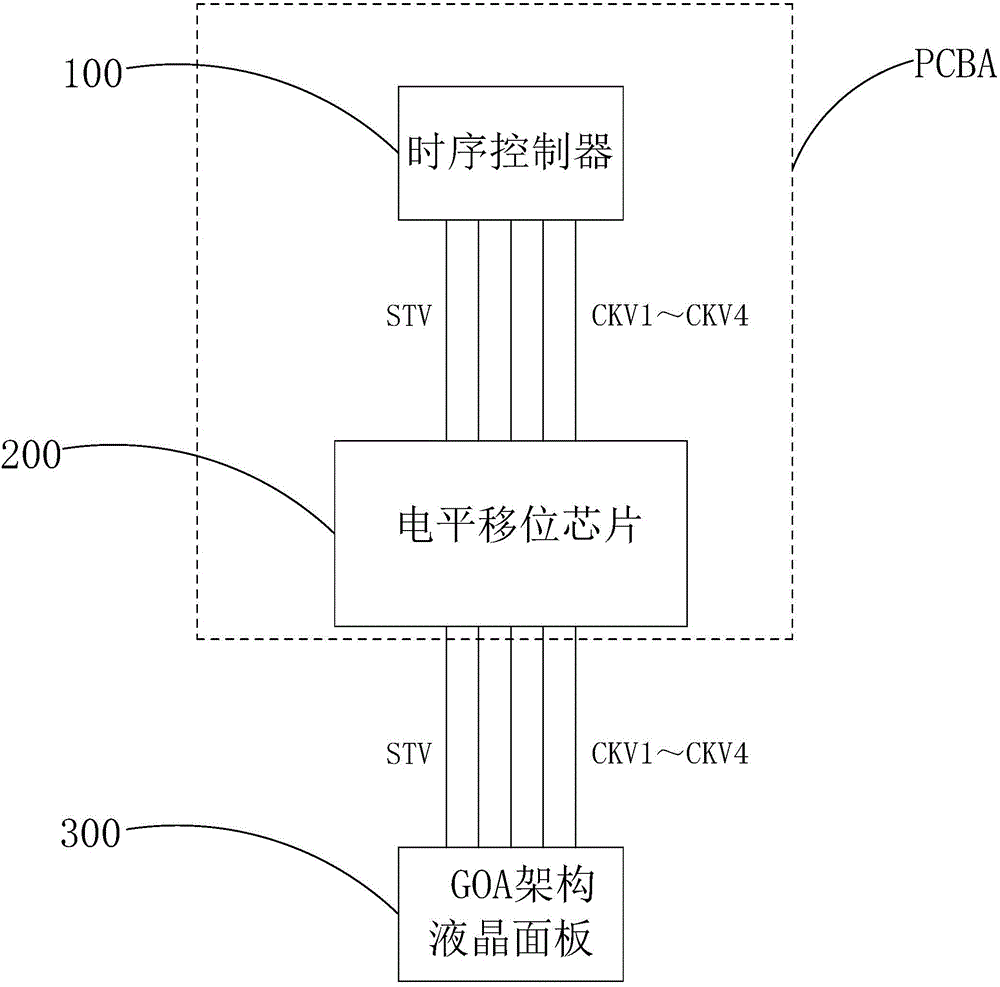
[0040] Please also see Figure 4 , Figure 5 ,and Figure 6 , the present invention provides a level shifting circuit for a GOA structure liquid crystal panel. The level shifting circuit for the GOA structure liquid crystal panel includes: a timing controller 10 and a level shifting chip 20, and the timing controller 10 and a level shifting chip 20 are arranged on the circuit driving board PCBA.

[0041] The level shift chip 20 includes a delay calculation register module 201 .

[0042] The timing controller 10 is communicatively connected with the level shift chip 20 through the start signal line 30 and the IIC bus 40 .

[0043] The IIC bus 40 includes a serial data signal line for transmitting the serial data signal SDA and a serial timing s...


PUM


Abstract

The invention provides a level shifting circuit and method for a GOA-framework liquid crystal panel. A delay calculation and registration module (201) is arranged inside a level shifting chip (20); a time sequence controller (10) is in communication connection with the level shifting chip (20) through a start signal line (30) and an IIC bus (40); the time sequence controller (10) performs initialized assignment (T1-Tn) on the delay calculation and registration module (201) through the IIC bus (40), and sends a start signal (STV) to the level shifting chip (20) through the start signal line (30); with the start signal (STV) as a reference, the level shifting chip (20) triggers to output at least four groups of time sequence signals (CKV1-CKVn) according to the initialized assignment (T1-Tn) in the delay calculation and registration module, and boosts the start signal (STV) and the voltages of at least four groups of time sequence signals (CKV1-CKVn)) so as to drive the GOA-framework liquid crystal panel (50), so that more time sequence signals are generated at the relatively low cost.

Description

technical field [0001] The invention relates to the field of display technology, in particular to a level shift circuit and a level shift method for a GOA structure liquid crystal panel. Background technique [0002] Active Matrix Liquid Crystal Display (AMLCD) is currently the most commonly used display device, the active matrix liquid crystal display includes a plurality of pixels, each pixel has a thin film transistor (Thin Film Transistor, TFT), the The gate of the TFT is connected to the scanning line extending in the horizontal direction, the drain of the TFT is connected to the data line extending in the vertical direction, and the source of the TFT is connected to the corresponding pixel electrode. If enough positive voltage is applied to a scanning line in the horizontal direction, all TFTs connected to the scanning line will be turned on, and the data signal voltage loaded on the data line will be written into the pixel electrode, thereby displaying the picture . ...

Claims


Application Information

Patent Timeline
Patent Type & Authority Applications(China)
IPC IPC(8): G09G3/36
CPCG09G3/3677G09G2300/0408G09G3/3648G09G2310/0289G09G2330/021
Inventor 曾德康徐枫程吴晶晶
Owner TCL CHINA STAR OPTOELECTRONICS TECH CO LTD
Why Eureka
Try Eureka