A kind of microstructure layer and light emitting diode

A microstructure layer and microsphere technology, applied in thin material processing, electrical components, nanotechnology, etc., can solve the problems of difficulty in obtaining nanometer-scale microspheres, difficult to achieve, etc., and achieve the effect of improving light extraction efficiency and not easy to fall off.

Active Publication Date: 2018-09-11
TSINGHUA UNIV +1
View PDF6 Cites 0 Cited by
  • Summary
  • Abstract
  • Description
  • Claims
  • Application Information

AI Technical Summary

Problems solved by technology

However, it is difficult to obtain nanometer-sized microspheres by first evaporating or depositing a metal layer, and then etching. It is difficult to achieve oriented arrays of nanometer-sized microparticles, and the distance between microparticles is small.

Method used


Image

  • A kind of microstructure layer and light emitting diode
  • A kind of microstructure layer and light emitting diode
  • A kind of microstructure layer and light emitting diode

Examples


Embodiment Construction

[0022] Various embodiments of the nanoscale microstructure and its preparation method will be further described in detail below in conjunction with the accompanying drawings.

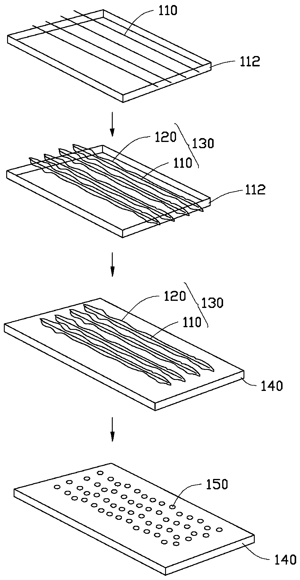
[0023] see figure 1 , the first embodiment of the present invention provides a method for preparing a nanoscale microstructure, which includes the following steps:

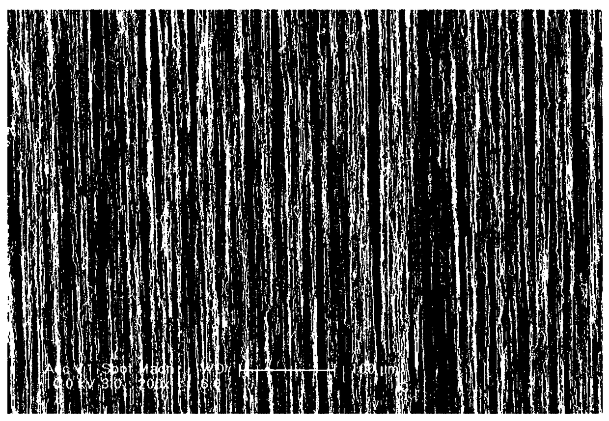
[0024] Step S10, providing a carbon nanotube structure 110, the carbon nanotube structure 110 comprising a plurality of carbon nanotubes arranged in an orderly manner;

[0025] Step S20, setting the carbon nanotube structure 110 in the air;

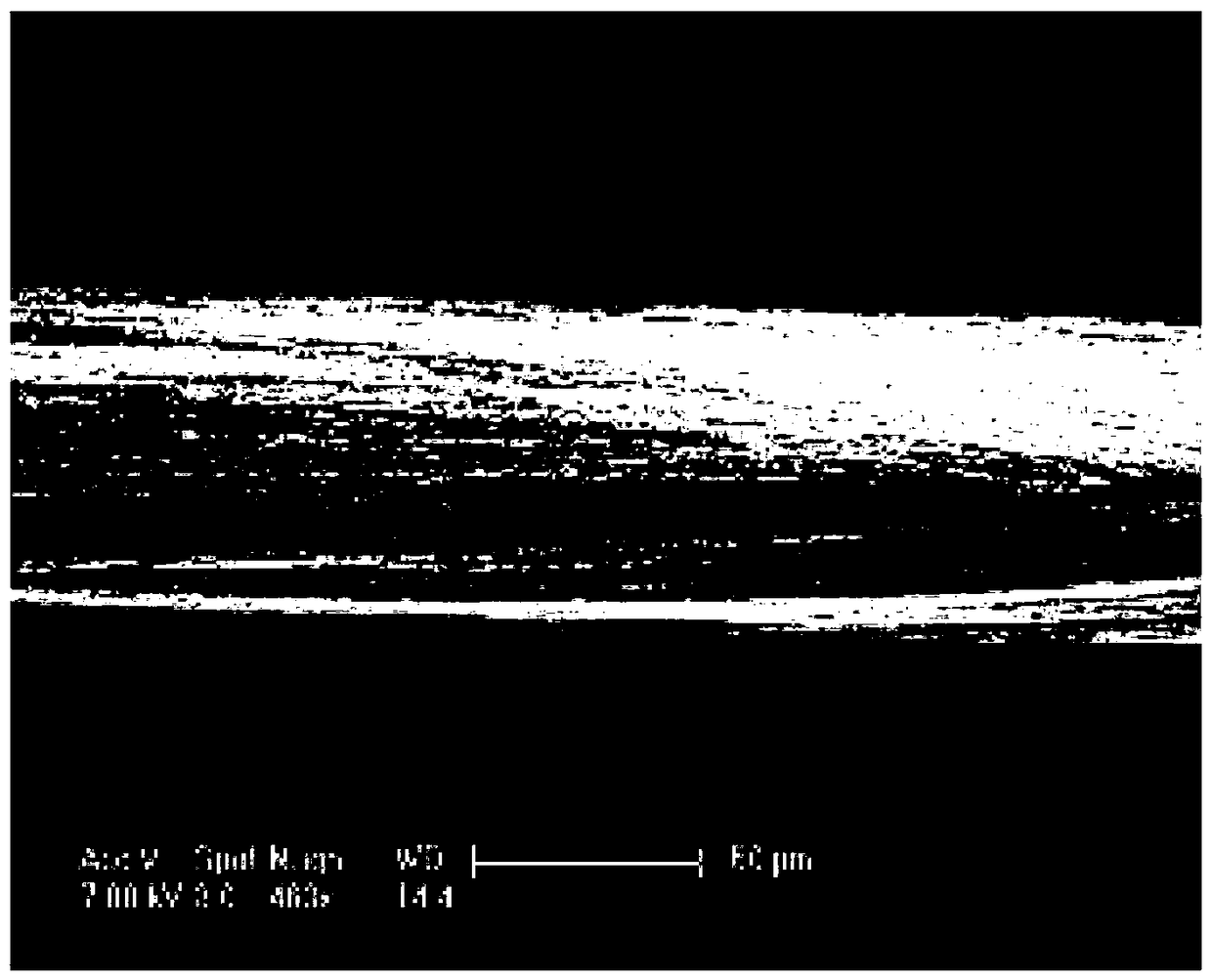
[0026] Step S30, setting a prefabricated layer 120 on the surface of the carbon nanotube structure 110, so that the thickness of the prefabricated layer 120 on the surface of each carbon nanotube is 2 nanometers to 10 nanometers, so as to obtain a carbon nanotube composite structure 130;

[0027] Step S40, transferring the carbon nanotube composite structure 130 to the surface of a substrate 140, and...


PUM

PropertyMeasurementUnit
sizeaaaaaaaaaa
sizeaaaaaaaaaa
sizeaaaaaaaaaa

Abstract

A nanostructure layer includes a number of nanostructures, wherein the number of nanostructures are aligned along a number of straight lines, a size of each of the number of nanostructures ranges from about 20 nanometers to about 100 nanometers, a distance between adjacent two nanostructures ranges from about 10 nanometers to about 300 nanometers, and each of the number of nanostructures includes a core and a shell coated on the core. A light emitting diode with the nanostructure layer is also provided.

Description

technical field [0001] The invention relates to a microstructure layer and a light-emitting diode, in particular to a nanoscale microstructure and the application of the microstructure to the light-emitting diode. Background technique [0002] In the prior art, when making various semiconductor devices, it is often necessary to make microstructures with tens of nanometers to hundreds of nanometers. However, it is difficult to obtain nanometer-sized microspheres by first evaporating or depositing a metal layer, and then etching. It is difficult to achieve oriented arrangement of nanometer-sized microparticles with a small distance between microparticles. Contents of the invention [0003] In view of this, it is indeed necessary to provide a microstructure layer, the size and spacing of the microspheres in the microstructure layer are both nanoscale. [0004] A microstructure layer, which is composed of a plurality of microspheres spaced apart from each other, and the plura...

Claims


Application Information

Patent Timeline
Patent Type & Authority Patents(China)
IPC IPC(8): H01L33/48H01L33/00B82Y30/00
CPCH01L33/42H01L2933/0091Y10T428/268
Inventor 金元浩李群庆范守善
Owner TSINGHUA UNIV
Why Eureka
Try Eureka