A method for fabricating a thin film transistor

A technology of thin-film transistors and oxide semiconductors, which is applied in the manufacture of transistors, semiconductor devices, semiconductor/solid-state devices, etc., can solve the problems of limited material combinations, achieve improved resolution, low sub-threshold slope, and reduce the size of transistors.

Inactive Publication Date: 2015-06-03
INTERUNIVERSITAIR MICRO ELECTRONICS CENT (IMEC VZW) +2
View PDF3 Cites 8 Cited by
  • Summary
  • Abstract
  • Description
  • Claims
  • Application Information

AI Technical Summary

Problems solved by technology

However, it is challenging to find etchants that provide good etch selectivity between metal and metal-oxide-semiconductor layers, which limits the material combinations that can be used.

Method used


Image

  • A method for fabricating a thin film transistor
  • A method for fabricating a thin film transistor
  • A method for fabricating a thin film transistor

Examples


Embodiment Construction

[0027] Detailed Description of Preferred Embodiments

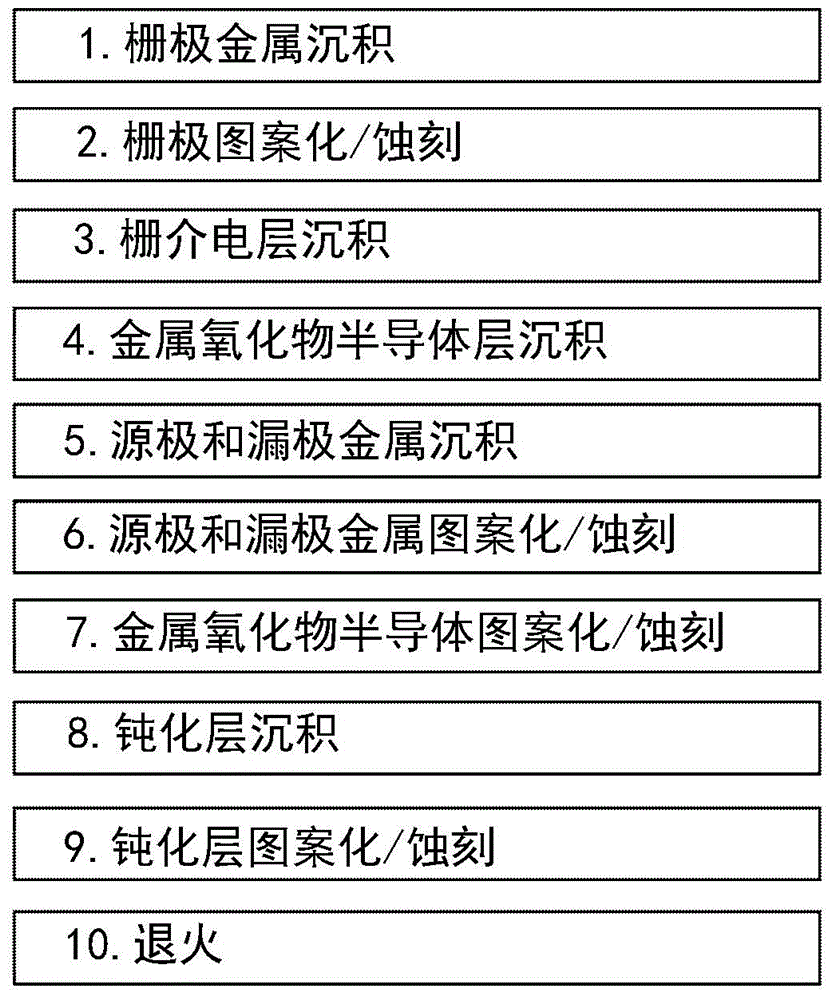
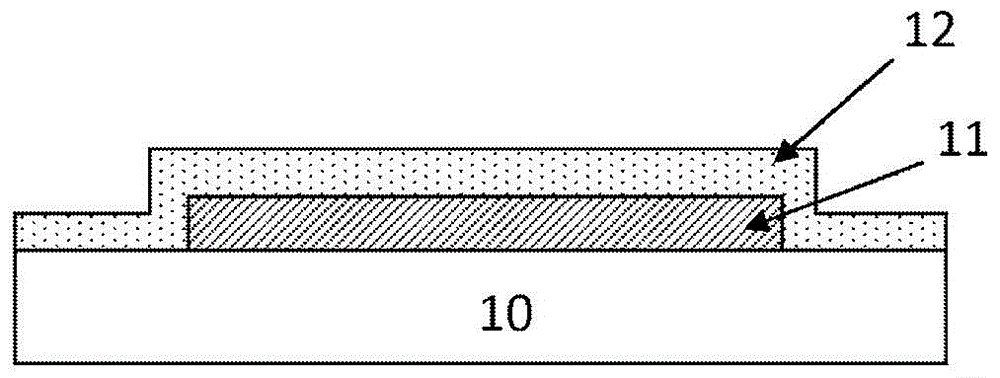
[0028] In the following detailed description, numerous specific details are set forth in order to provide a thorough understanding of the invention and practice of specific embodiments. However, it is understood that the invention may be practiced without these specific details. In other instances, well-known methods, procedures and techniques have not been described in detail so as not to obscure the present invention. While the invention has been described in terms of particular embodiments and with reference to certain drawings, the invention is not limited thereto. The drawings included and described herein are schematic and do not limit the scope of the invention. It should also be noted that in the drawings, the size of some of the elements may be exaggerated for illustrative purposes and therefore not drawn on scale.

[0029] Moreover, the terms "first", "second", "third", etc. in the specification are used to di...


PUM

PropertyMeasurementUnit
thicknessaaaaaaaaaa
thicknessaaaaaaaaaa
thicknessaaaaaaaaaa

Abstract

A method for fabricating a bottom-gate top-contact metal oxide semiconductor thin film transistor, the method comprising: - forming a gate electrode on a substrate; - providing a gate dielectric layer covering the gate electrode; - depositing a metal oxide semiconductor layer on the gate dielectric layer; - depositing a metal layer on top of the metal oxide semiconductor layer; - patterning said metal layer to form source and drain contacts, wherein patterning the metal layer comprises dry etching of the metal layer; and thereafter patterning the metal oxide semiconductor layer.

Description

field of invention [0001] The technology of the present invention relates to a method for fabricating a metal oxide semiconductor thin film transistor, more specifically to a method for fabricating a metal oxide semiconductor bottom-gate top-contact thin film transistor, and also relates to the thin film transistor obtained therefrom. technical background [0002] Metal oxide semiconductors have found application in thin film electronics such as large area displays and circuits because of their ability to achieve excellent electrical properties at low processing temperatures. For example, a thin film transistor (TFT) using amorphous gallium-indium-zinc-oxide (a-GIZO) as an active layer has been demonstrated. Achieving excellent mobility (μ) and excellent threshold voltage (V TH ) control is an important parameter. [0003] In processes for fabricating bottom gate top contact (BGTC) metal oxide semiconductor thin film transistors, an etch stop layer is often used to protect...

Claims


Application Information

Patent Timeline
Patent Type & Authority Applications(China)
IPC IPC(8): H01L29/66H01L29/786
CPCH01L29/66742H01L29/786H01L29/7869H01L29/66969H01L21/3065
Inventor M·纳格S·斯台德
Owner INTERUNIVERSITAIR MICRO ELECTRONICS CENT (IMEC VZW)
Why Eureka
Try Eureka