Manufacturing technology of groove MOSFET device with masking films of decreased number

A manufacturing process and trench technology, applied in the field of semiconductor device manufacturing, can solve problems such as device defects and achieve the effect of reducing the number of masks

Inactive Publication Date: 2010-03-17
KEDA SEMICON
View PDF0 Cites 9 Cited by
  • Summary
  • Abstract
  • Description
  • Claims
  • Application Information

AI Technical Summary

Problems solved by technology

[0003] The existing trench MOSFET manufacturing process includes many photolithographic masking processes and mask

Method used


Image

  • Manufacturing technology of groove MOSFET device with masking films of decreased number
  • Manufacturing technology of groove MOSFET device with masking films of decreased number
  • Manufacturing technology of groove MOSFET device with masking films of decreased number

Examples


Embodiment Construction

[0038] Embodiments of the present invention will be described in detail below in conjunction with the accompanying drawings.

[0039] Refer to the following Figure 1 to Figure 13 A preferred example described further illustrates the trench MOSFET manufacturing method of the present invention, so as to better understand the present invention and its advantages.

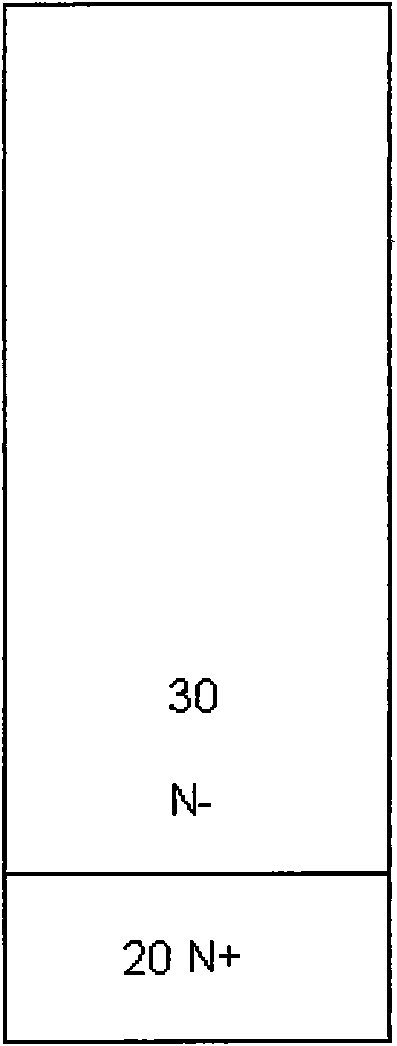
[0040] figure 1 Shown is a schematic of a pristine silicon wafer. exist figure 1 Among them, the original silicon wafer substrate 20 can adopt N+(100) crystal orientation, the resistivity is 0.001~0.002ohm*cm, and the epitaxial layer 30N-silicon polished wafer with resistivity 0.1~10ohm*cm;

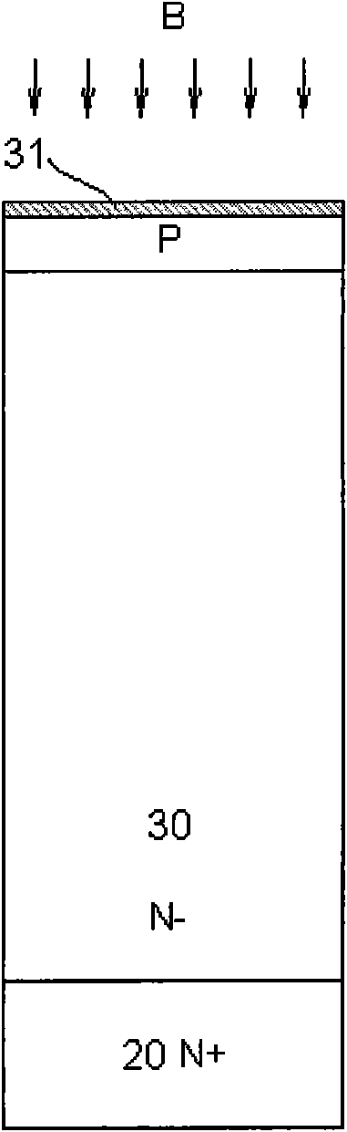
[0041] First, an oxide layer 31 of about 200-800 Å is grown on the silicon material as a pre-implantation oxide layer; then, boron is implanted into the entire silicon wafer. Such as figure 2 shown.

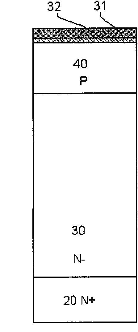
[0042] Then deposit a layer of silicon nitride or oxide layer 32 with a thickness of about 200-5000A, and then advance the ...


PUM

PropertyMeasurementUnit
Thicknessaaaaaaaaaa
Thicknessaaaaaaaaaa

Abstract

The invention relates to a manufacturing technology of a groove MOSFET device with masking films of a decreased number, which is characterized by comprising the following steps: selecting a substratematerial; growing an epitaxial layer on the substrate material; forming a trap area; forming a groove; growing a gate oxide in an oxidizing way; depositing polysilicon, and sculpturing the polysilicon; forming an N+ area. depositing an isolation medium layer; sculpturing a contact hole, and forming a P+ area; depositing a metal layer, and then photoengraving and sculpturing metal, thus the numberof the masking films of the produced groove MOSFET device is decreased to four.

Description

Technical field: [0001] The invention belongs to the field of semiconductor device manufacturing, and in particular relates to a manufacturing process for trench MOSFET devices with reduced number of masks. Background technique: [0002] With the development of power electronics technology, the application of power MOSFET devices is becoming more and more extensive. In order to achieve better device performance, a trench-structured MOSFET appears. Trench technology changes the conductive channel of MOSFET from horizontal to vertical, increases the cell density, and improves the current handling capacity of power devices. [0003] The existing trench MOSFET manufacturing process includes many photolithography mask processes and mask alignment processes, each process requires production time and cost, and each process may generate device defects. Reducing the number of masks and process steps required to produce devices can reduce production costs and increase product yield....

Claims


Application Information

Patent Timeline
IPC IPC(8): H01L21/336
Inventor 陈智勇向军利胥超
Owner KEDA SEMICON
Why Eureka
Try Eureka