Manufacturing method of array substrate of semi-reflection semi-penetration liquid crystal display

A semi-reflective, semi-transmissive, liquid crystal display technology, used in semiconductor/solid-state device manufacturing, instruments, photolithography process exposure devices, etc. The effect of increasing the aperture ratio

Active Publication Date: 2006-11-29
AU OPTRONICS CORP
View PDF0 Cites 9 Cited by
  • Summary
  • Abstract
  • Description
  • Claims
  • Application Information

AI Technical Summary

Problems solved by technology

Among the three processes, the production cost of photolithography is the highest

Method used


Image

  • Manufacturing method of array substrate of semi-reflection semi-penetration liquid crystal display
  • Manufacturing method of array substrate of semi-reflection semi-penetration liquid crystal display
  • Manufacturing method of array substrate of semi-reflection semi-penetration liquid crystal display

Examples


Embodiment 1

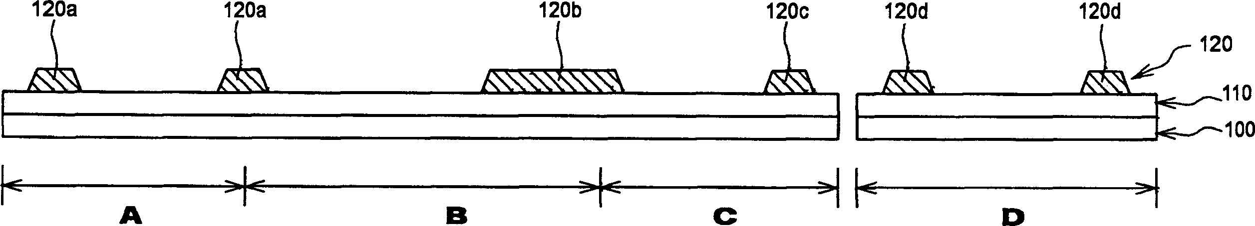
[0021] Figures 1A-1G It is a cross-sectional view of each process stage of the array substrate of the transflective liquid crystal display according to a preferred embodiment of the present invention. see first Figure 1A , from left to right are structural cross-sectional views of the thin film transistor region A, the pixel region B, the storage capacitor region C, and the gate pad region D in sequence. First, the transparent conductive layer 110 and the first metal layer 120 are sequentially formed on the substrate 100 . Then use a first half-tone mask to define the first metal layer 120 and the transparent conductive layer 110 at the same time, so that the first metal layer 120 forms complementary patterns of gates, capacitor lines, scan lines (not shown) and gate pads 120a, 120c, 120d, at the same time, a reflective layer 120b is formed on the reflective part of the pixel region B, and the transparent conductive layer 110 is formed as a pixel electrode. The complementa...

Embodiment 2

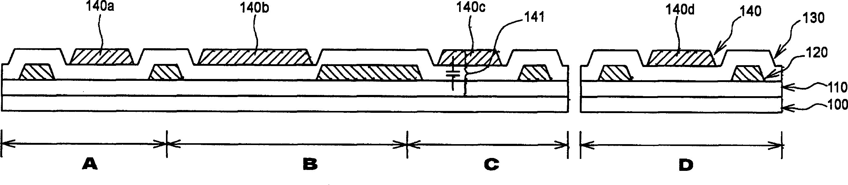
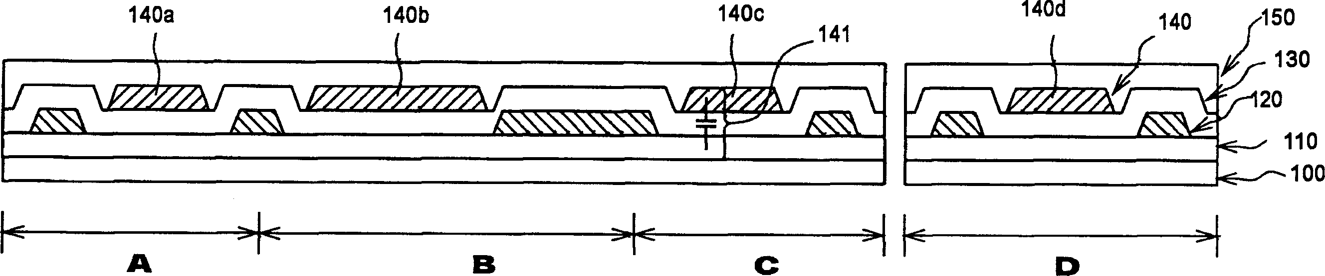
[0030] Figures 2A-2D It is a cross-sectional view of each process stage of the array substrate of the transflective liquid crystal display according to another preferred embodiment of the present invention. The steps from the formation of the transparent conductive layer to the formation of the dielectric layer in the second embodiment are substantially the same as those in the first embodiment, so the related descriptions of FIGS. 1A-1C can be directly referred to.

[0031] See Figure 2A , after the dielectric layer 150 is formed, a second mask is used to define the dielectric layer 150, the second metal layer 140 and the first protective layer 130 at the same time. In this step, the sacrificial metal layer 140b and the dielectric layer 150 structure on the penetrating portion of the pixel region B are removed, and the dielectric layer 150 and the first protective layer above the side of the first storage capacitor 141 are removed at the same time 130 to form the contact ...


PUM


Abstract

A method for preparing array base plate of semireflection-semitransmission liquid crystal display includes forming transparent conductive layer, the first metal layer, the first protective layer and the second metal layer in sequence on substrate then forming a dielectric layer on substrate; removing off dielectric layer and second metal layer as well as the first protective layer at certain positions to form a channel region above dielectric layer; forming the third metal layer and the second protective layer on base plate; defining three said metal layers and two protective layers as well as transparent layer in following their forming process correspondingly.

Description

technical field [0001] The invention relates to a method for manufacturing a liquid crystal display, in particular to a method for manufacturing an array substrate of a semi-reflective and semi-transparent liquid crystal display. Background technique [0002] Recently, the continuous innovation of optoelectronic technology, coupled with the arrival of the digital age, has promoted the vigorous development of the liquid crystal display market. Liquid crystal displays have many advantages such as high image quality, small size, light weight, low driving voltage and low power consumption. Therefore, it is widely used in consumer communication or electronic products such as personal digital assistants (PDAs), mobile phones, camcorders, notebook computers, desktop monitors, car monitors and projection TVs, and gradually replaces cathode rays. tube, and become the mainstream of the display. [0003] At present, the manufacturing method of the thin film transistor array (TFT Arra...

Claims


Application Information

Patent Timeline
Patent Type & Authority Applications(China)
IPC IPC(8): G02F1/1333G03F7/20H01L21/00
Inventor 林士杰
Owner AU OPTRONICS CORP
Why Eureka
Try Eureka