

Semiconductor device and method of manufacturing the same
a semiconductor device and semiconductor technology, applied in the direction of semiconductor devices, electrical devices, transistors, etc., can solve the problems of unstable difficult to reduce the device size of npn transistors, and difficult to obtain desired breakdown voltage characteristics of npn transistors, etc., to improve the breakdown voltage characteristics of semiconductor devices, reduce device size, and improve the effect of semiconductor device breakdown voltage characteristics
- Summary
- Abstract
- Description
- Claims
- Application Information
AI Technical Summary
Benefits of technology
Problems solved by technology
Method used
Image

Examples
Embodiment Construction
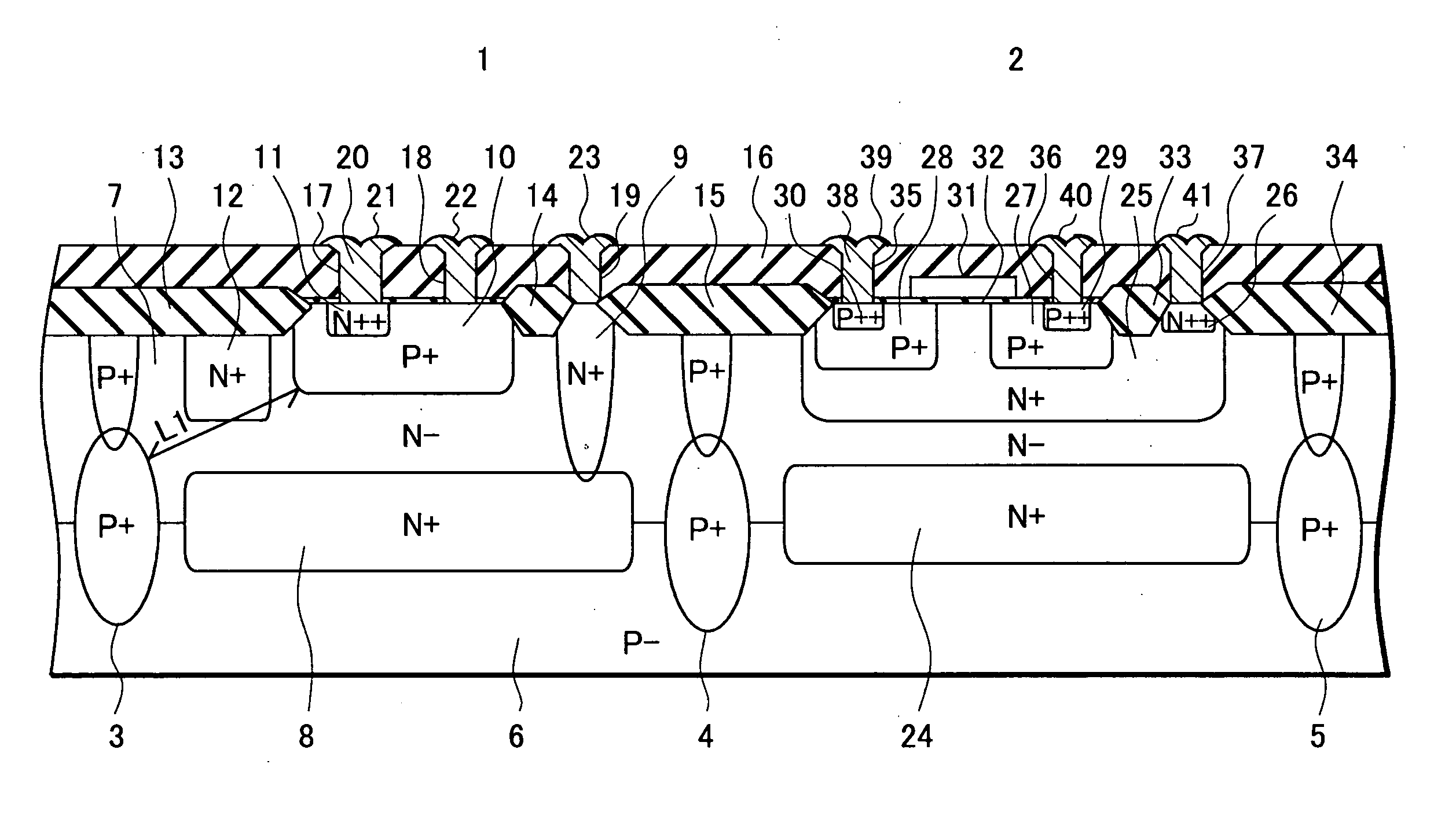
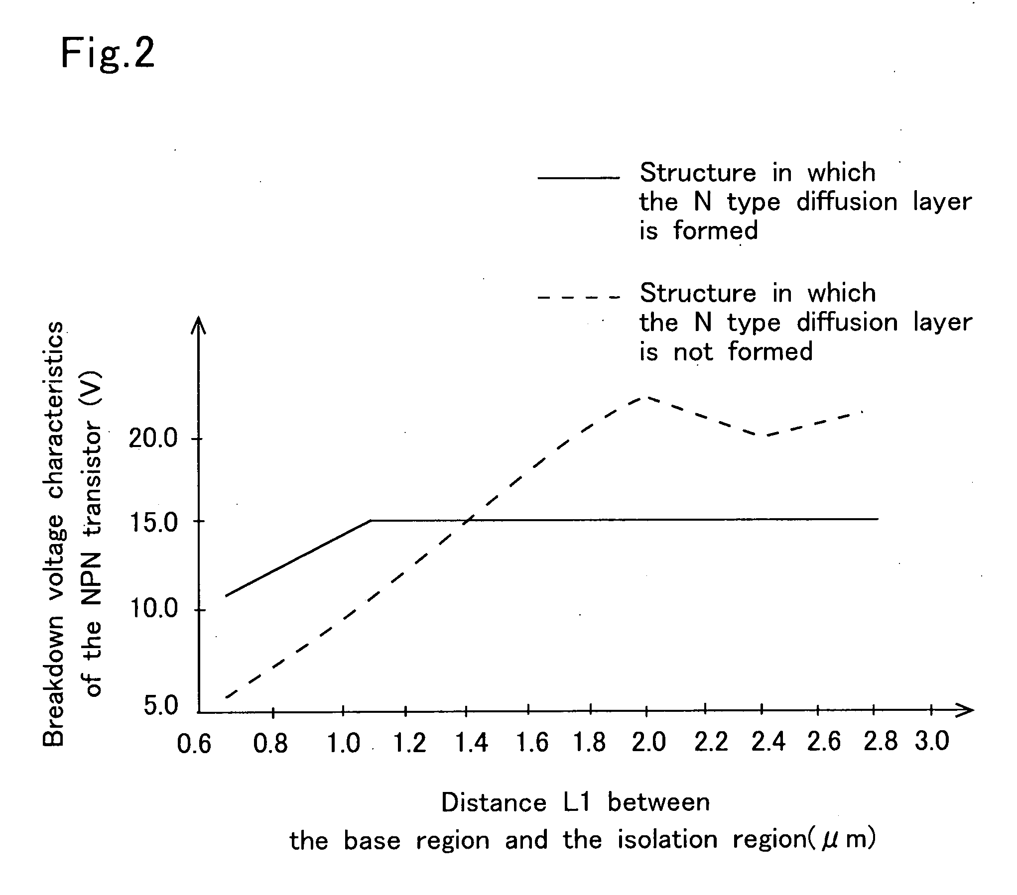
[0033] By referring to FIGS. 1 and 2, detailed descriptions will be provided below for a first example of a semiconductor device according to an embodiment of the present invention. FIG. 1 is a cross-sectional view illustrating the semiconductor device of the embodiment. FIG. 2 is a graph illustrating breakdown voltage characteristics of the semiconductor device of the embodiment.
[0034] As shown in FIG. 1, an NPN transistor 1 is formed in one of element formation regions divided by isolation regions 3, 4 and 5, and a P channel MOS (Metal Oxide Semiconductor) transistor 2 is formed in a different element formation region. Note that, although not shown in FIG. 1, an N channel MOS transistor, a PNP transistor and the like are formed in other element formation regions.
[0035] As shown in FIG. 1, the NPN transistor 1 is mainly formed of a P type single crystal silicon substrate 6, an N type epitaxial layer 7, an N type buried diffusion layer 8 used as a collector region, an N type diffu...
PUM
 Abstract
Description
Claims
Application Information