Semiconductor device and manufacturing method of the same

a technology of semiconductors and semiconductors, applied in semiconductor devices, electrical devices, transistors, etc., can solve the problem of difficult short-circuit between the base region and the isolation region, and achieve the effect of reducing the size of the device, and improving the breakdown voltage characteristics

Inactive Publication Date: 2007-06-28
SEMICON COMPONENTS IND LLC
View PDF14 Cites 10 Cited by
  • Summary
  • Abstract
  • Description
  • Claims
  • Application Information

AI Technical Summary

Benefits of technology

[0009] Moreover, the semiconductor device of the present invention includes the first diffusion layer of one conductivity type is surrounded by the first diffusion layer of the opposite conductivity type and the third diffusion layer of the opposite conductivity type. In the present invention, therefore, the diffusion layers of the opposite conductivity type surround the base region of the one conductivity type. Use of this structure makes it hard for the short-circuit to occur between the base region and the isolation region. Thus, the breakdown voltage characteristics can be improved.
[0010] Moreover, the semiconductor device of the present invention further includes a buried diffusion layer of the one conductivity type which forms the isolation region, which is formed from a surface of the first epitaxial layer, and which is connected to the semiconductor substrate, and a second diffusion layer of the one conductivity type which forms the isolation region, which is formed from a surface of the second epitaxial layer, and which is connected to the buried diffusion layer of the one conductivity type. In the present invention, therefore, lateral expansion of the buried diffusion layer of the one conductivity type, which forms the isolation region, is suppressed. Thus, a device size can be reduced.
[0011] A method of manufacturing a semiconductor device according to the present invention includes the steps of: preparing a semiconductor substrate of one conductivity type, forming a first buried diffusion layer of an opposite conductivity type and a second buried diffusion layer of the opposite conductivity type in the semiconductor substrate, and thereafter forming an first epitaxial layer of the opposite conductivity type on the semiconductor substrate, implanting ions of impurities of the one conductivity type in a desired region of the first epitaxial layer, thereafter forming a second epitaxial layer of the opposite conductivity type on the first epitaxial layer, and forming a buried diffusion layer of the one conductivity type so as to expand in the first and second epitaxial layers, forming a first diffusion layer of the opposite conductivity type, which is used as a collector region, in the second epitaxial layer, forming a first diffusion layer of the one conductivity type, which is used as a base region, in the second epitaxial layer, forming a second diffusion layer of the opposite conductivity type, which is used as an emitter region, in the first diffusion layer of the one conductivity type, forming a second diffusion layer of the one conductivity type, which is connected to the buried diffusion layer of the one conductivity type, in the second epitaxial layer, forming, in the second epitaxial layer, a third diffusion layer of the opposite conductivity type, which is disposed between the first diffusion layer of the one conductivity type and the second diffusion layer of the one conductivity type, and a fourth diffusion layer of the opposite conductivity type, which is used as a back gate region, by the same ion implantation step, and forming, in the fourth diffusion layer of the opposite conductivity type, a third diffusion layer of the one conductivity type, which is used as a source region, and a fourth diffusion layer of the one conductivity type, which is used as a drain region. In the present invention, therefore, the third diffusion layer of the opposite conductivity type, which improves breakdown voltage characteristics, and the fourth diffusion layer of the opposite conductivity type, which is used as the back gate region, are formed by the same step. This manufacturing method enables reduction in the number of masks and reduction in manufacturing costs.
[0012] Moreover, the method of manufacturing a semiconductor device according to the present invention includes the second epitaxial layer is formed so as to have an impurity concentration higher than that of the first epitaxial layer. In the present invention, therefore, the breakdown voltage characteristics can be improved by increasing the impurity concentration of the second epitaxial layer and by this making it hard for a short-circuit to occur between the base region and the isolation region.
[0013] Moreover, the method of manufacturing a semiconductor device according to the present invention includes, after the second epitaxial layer is formed, an ion implantation step for forming the second diffusion layer of the one conductivity type is performed without performing a thermal diffusion step for expanding the buried diffusion layer of the one conductivity type. In the present invention, therefore, by controlling a thickness of the first epitaxial layer so that the dedicated thermal diffusion step for the buried diffusion layer of the one conductivity type can be omitted, the lateral expansion width of the buried diffusion layer of the one conductivity type can be suppressed.
[0014] Moreover, the method of manufacturing a semiconductor device according to the present invention includes, after a LOCOS oxide film is formed in the second epitaxial layer, ions of impurities of the one conductivity type for forming the second diffusion layer of the one conductivity type are implanted from a surface of the LOCOS oxide film. In the present invention, therefore, it is possible to reduce crystal defects in a formation region of the second diffusion layer of the one conductivity type.

Problems solved by technology

Use of this structure makes it hard for the short-circuit to occur between the base region and the isolation region.

Method used


Image

  • Semiconductor device and manufacturing method of the same
  • Semiconductor device and manufacturing method of the same
  • Semiconductor device and manufacturing method of the same

Examples


Embodiment Construction

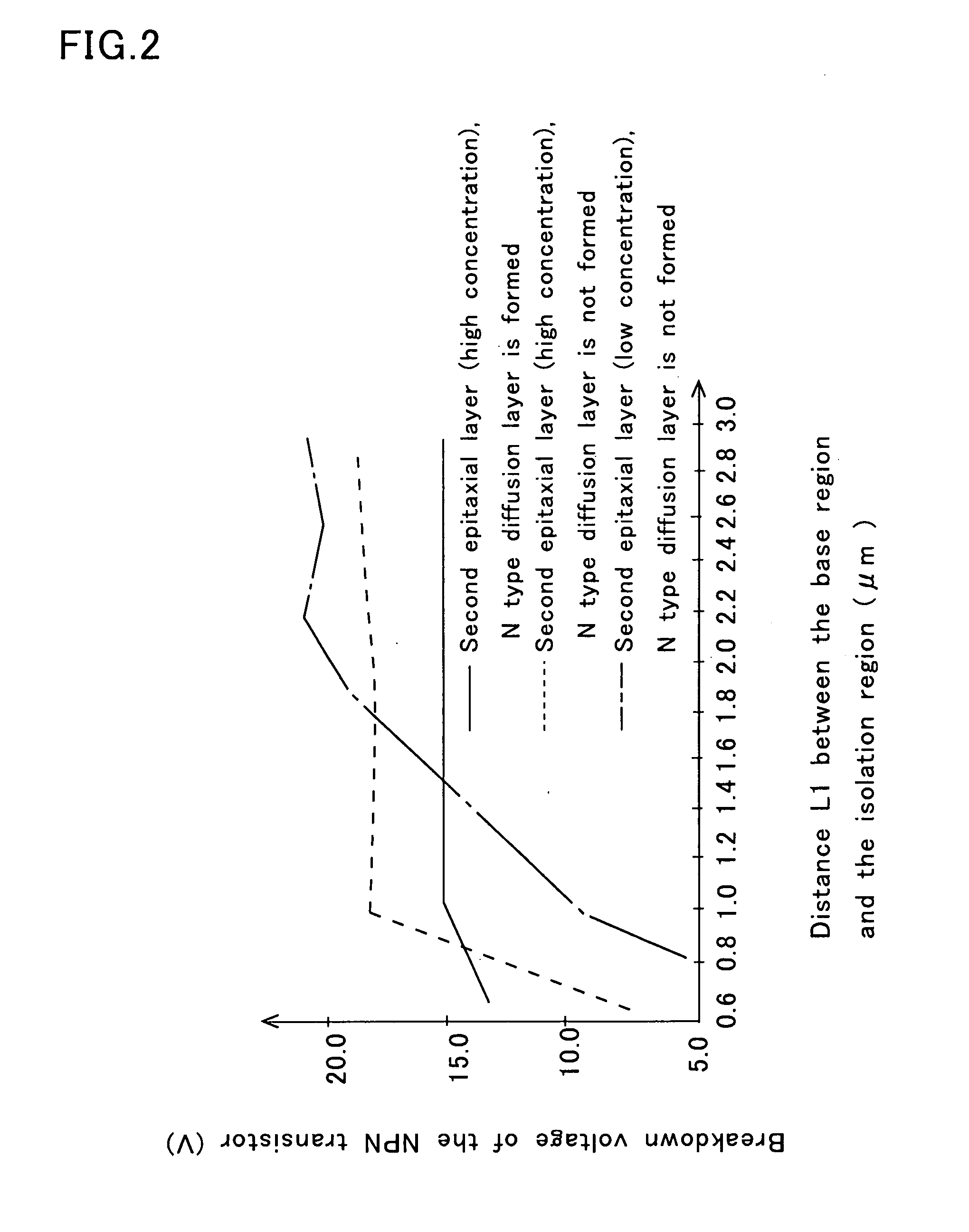
[0024] With reference to FIGS. 1 and 2, a semiconductor device according to an embodiment of the present invention will be described in detail below. FIG. 1 is a cross-sectional view illustrating the semiconductor device according to this embodiment. FIG. 2 is a graph illustrating breakdown voltage characteristics of the semiconductor device according to this embodiment.

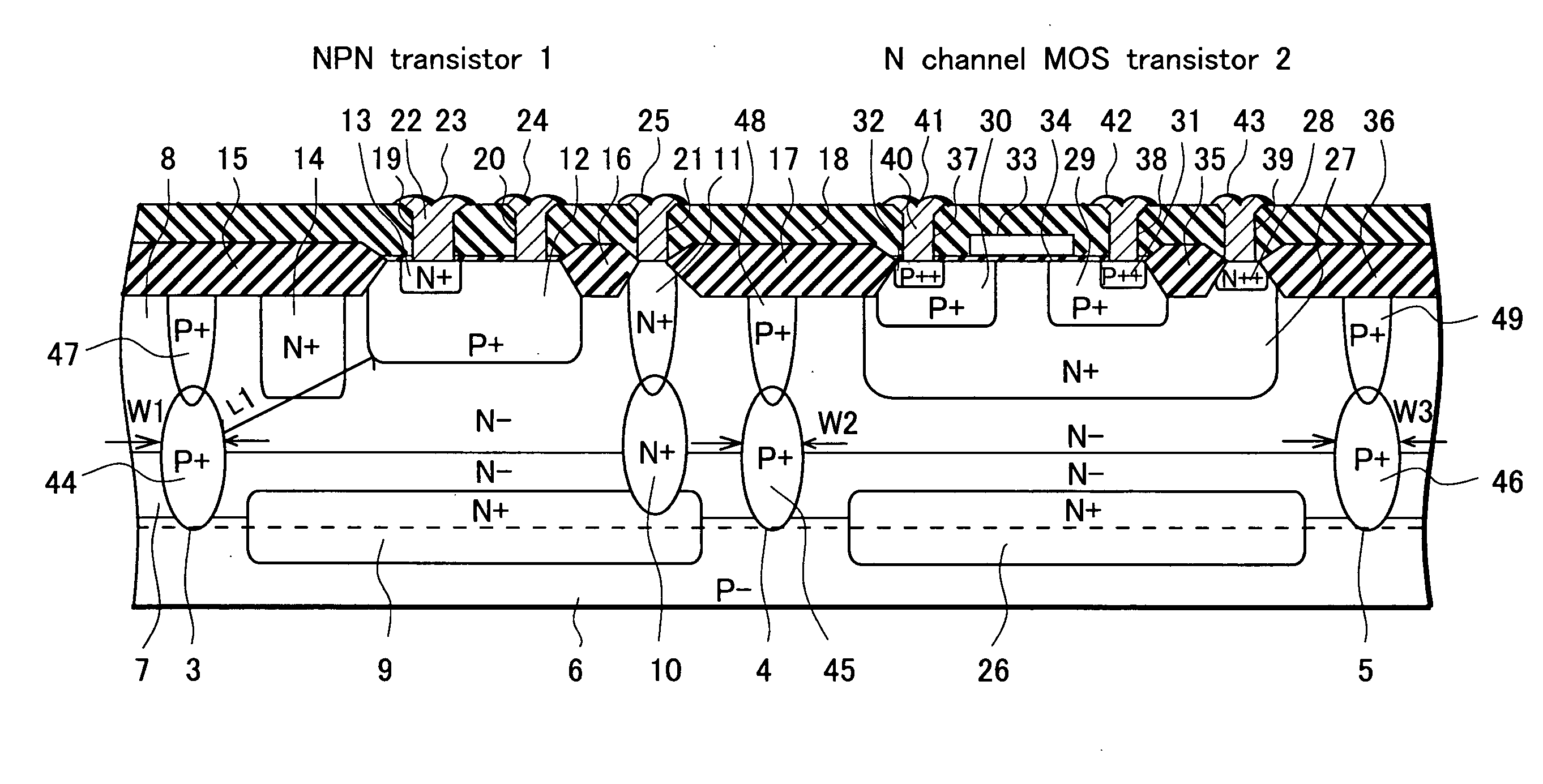
[0025] As shown in FIG. 1, an NPN transistor 1 is formed in one of element formation regions divided by isolation regions 3, 4 and 5, and an N channel MOS (Metal Oxide Semiconductor) transistor 2 is formed in another element formation region. Note that, although not shown in FIG. 1, a P channel MOS transistor, a PNP transistor and the like are formed in other element formation regions.

[0026] As shown in FIG. 1, the NPN transistor 1 is mainly configured of: a P type single crystal silicon substrate 6, N type epitaxial layers 7 and 8, N type buried diffusion layers 9 and 10 used as a collector region, an N type diffu...


PUM


Abstract

In a semiconductor device of the present invention, two epitaxial layers are formed on a P type single crystal silicon substrate. One of the epitaxial layers has an impurity concentration higher than that of the other epitaxial layer. The epitaxial layers are divided into a plurality of element formation regions by isolation regions. In one of the element formation regions, an NPN transistor is formed. Moreover, between a P type diffusion layer, which is used as a base region of the NPN transistor, and a P type isolation region, an N type diffusion layer is formed. Use of this structure makes it hard for a short-circuit to occur between the base region and the isolation region. Thus, the breakdown voltage characteristics of the NPN transistor can be improved.

Description

BACKGROUND OF THE INVENTION [0001] Priority is claimed to Japanese Patent Application Number JP2005-356008 filed on Dec. 9, 2005, the disclosure of which is incorporated herein by reference in its entirety. [0002] b 1. Field of the Invention [0003] The present invention relates to a semiconductor device which realizes reduction in a device size while maintaining breakdown voltage characteristics thereof, and a method of manufacturing the same. [0004] 2. Description of the Prior Art [0005] As an example of a conventional semiconductor device, a structure of the following NPN transistor 61 has been known. As shown in FIG. 9, an N type epitaxial layer 63 is formed on a P type semiconductor substrate 62. In the epitaxial layer 63, P type buried diffusion layers 64 and 65, which expand vertically (in a depth direction) from a surface of the substrate 62, and P type diffusion layers 66 and 67, which expand from a surface of the epitaxial layer 63, are formed. Moreover, the epitaxial layer...

Claims


Application Information

Patent Timeline
Patent Type & Authority Applications(United States)
IPC IPC(8): H01L29/00
CPCH01L21/8249H01L27/0623H01L29/0821H01L29/1004H01L29/66272H01L29/7322H01L29/7833H01L21/761H01L21/34H01L21/20
Inventor SOMA, MITSURUHATA, HIROTSUGUAKAISHI, MINORU
Owner SEMICON COMPONENTS IND LLC
Why Eureka
Try Eureka