Semiconductor device and manufacturing method thereof

A semiconductor and conductive semiconductor technology, applied in the manufacture of semiconductor/solid-state devices, semiconductor devices, transistors, etc., can solve problems such as deterioration of characteristics, and achieve the effect of preventing impact ionization and improving breakdown voltage characteristics

Inactive Publication Date: 2008-12-31
DONGBU HITEK CO LTD
View PDF0 Cites 4 Cited by
  • Summary
  • Abstract
  • Description
  • Claims
  • Application Information

AI Technical Summary

Problems solved by technology

Thus deteriorating the BV (breakdown voltage) characteristics

Method used


Image

  • Semiconductor device and manufacturing method thereof
  • Semiconductor device and manufacturing method thereof
  • Semiconductor device and manufacturing method thereof

Examples


Embodiment Construction

[0018] Hereinafter, semiconductor devices and methods of manufacturing the same according to embodiments will be described with reference to the accompanying drawings.

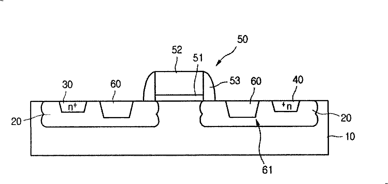
[0019] figure 1 is a cross-sectional view illustrating a semiconductor device according to an embodiment.

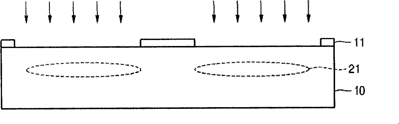
[0020] refer to figure 1 A drift region 20 containing N-type impurities is formed in the P-type semiconductor substrate 10 , and a source region 30 or a drain region 40 containing high-concentration N-type impurities is formed in the drift region 20 .

[0021] Then, a gate electrode 50 is formed between the drift regions 20 . The gate electrode 50 includes a gate insulating layer 51 , gate polysilicon 52 and spacers 53 .

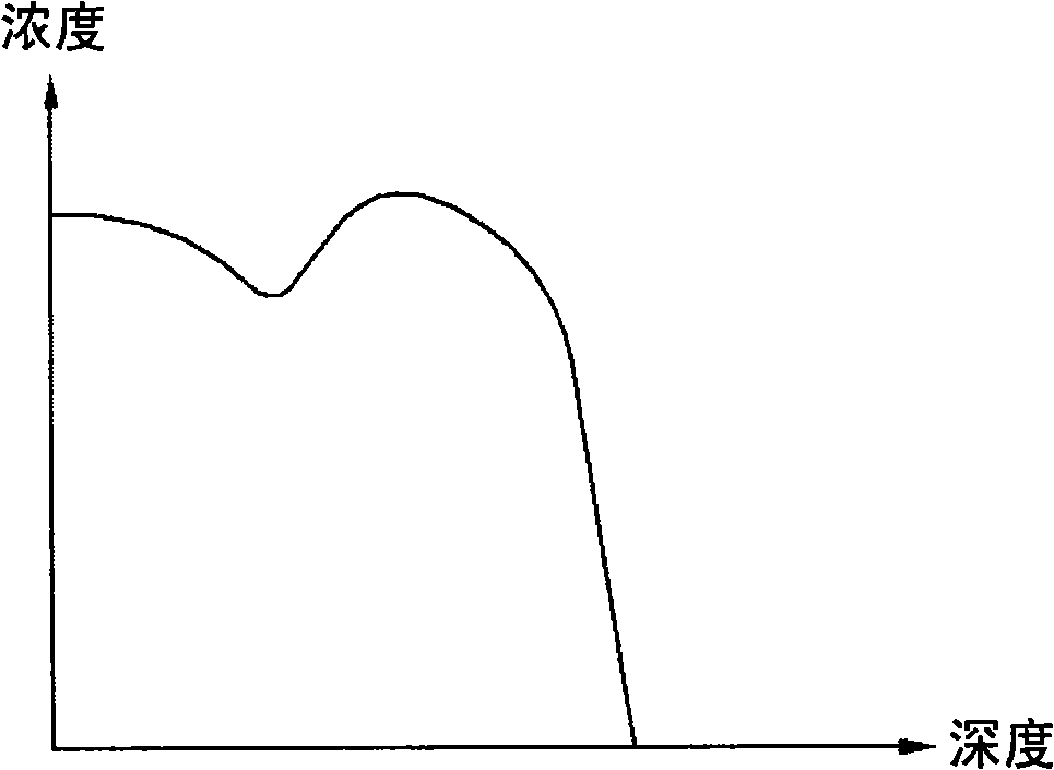
[0022] The drift region 20 is horizontally formed below the gate electrode 50 . Drift region 20 has a doping profile in which the impurity concentration gradually increases, then decreases, and again gradually increases, then decreases in a downward direction from the surface of se...


PUM


Abstract

The invention discloses a semiconductor device that can be used as a high voltage transistor. The semiconductor device can include a gate electrode on a semiconductor substrate, drift regions in the substrate at opposite sides of the gate electrode, a source region in one of the drift regions and a drain region in the other of the drift regions, and a shallow trench isolation (STI) region in a portion of the drift region between the gate electrode and the drain region. The portion of the drift region below the STI region can have a doping profile in which the concentration of impurities decreases from the concentration at the lower surface of the STI region, and then increases, and then again decreases. The invention improves puncture voltage characteristic of the semiconductor device, and collision ionization in the semiconductor device can be avoided.

Description

technical field [0001] The invention relates to a semiconductor device and a manufacturing method thereof. Background technique [0002] As semiconductor devices have been manufactured in small sizes, high voltage devices have also been gradually reduced in size. [0003] Specifically, high-voltage devices must perform the same regardless of their size. In addition, it is necessary to provide a manufacturing method compatible with the manufacturing process of low voltage devices. [0004] The breakdown phenomenon may occur in high voltage devices due to the snapback phenomenon. [0005] Specifically, if the voltage applied to the drain of a high voltage transistor is increased, electrons move from its source to the drain. Therefore, impact ionization may occur around the lower portion of the spacer located in the drain direction. [0006] As impact ionization occurs, holes move toward the substrate from the lower portion of the spacer located in the drain direction, caus...

Claims


Application Information

Patent Timeline
Patent Type & Authority Applications(China)
IPC IPC(8): H01L29/78H01L29/06H01L29/36H01L21/336
CPCH01L21/26513H01L29/0653H01L29/7833H01L29/0847H01L29/66568H01L29/0649H01L29/6659H01L29/66606H01L29/78
Inventor 金知泓张德基张炳琸朴盛羲
Owner DONGBU HITEK CO LTD
Why Eureka
Try Eureka