Analog switch circuit

a switch circuit and analog technology, applied in the field of analog switch circuits, can solve the problems of small voltage difference between a gate and a source, difficult operation of analog switches at low voltage, and the voltage between the gate and the source of an nmos transistor included in an analog switch may exceed the breakdown voltag

Inactive Publication Date: 2005-01-11
CYPRESS SEMICON CORP
View PDF8 Cites 6 Cited by
  • Summary
  • Abstract
  • Description
  • Claims
  • Application Information

AI Technical Summary

Benefits of technology

In order to achieve the above object, an analog switch circuit for sampling an analog signal is provided. This analog switch circuit comprises an analog switch section including a first n-channel MOS field effect transistor and a first p-channel MOS field effect transistor, sources of which are connected, drains of which are connected, and therefore which are connected in parallel, for inputting an analog input signal and for outputting a sampled analog output signal, a comparator circuit for inputting the analog input signal and a reference signal and for comparing the input potential of the analog input signal and the reference potential of the reference signal, and a voltage boost circuit for setting a potential of a gate of the first n-channel MOS field effect transistor to a potential of positive power supply voltage in the case of the input potential being lower than the reference potential at the time of the analog switch section being in a continuity state and for boosting the potential of the gate to a potential higher than the potential of the positive power supply voltage in the case of the input potential being higher than the reference potential at the time of the analog switch section being in a continuity state.

Problems solved by technology

Unlike digital circuits, however, the potential of the source and drain electrodes of metal oxide semiconductor (MOS) field effect transistors included in analog switches etc. used for sampling can be about half (VDD / 2) of power supply voltage (VDD) Therefore, voltage between a gate and a source is small compared with digital circuits and it is difficult for analog switches to operate at low voltage.
With the above conventional circuits, however, voltage between the gate and source of an NMOS transistor included in an analog switch may exceed the breakdown voltage, depending on circuit constants and operating conditions.
That is to say, at a minimum, input capacitance will roughly double, resulting in longer delay time.
As described above, with the conventional analog switch circuit 2, the original purpose is to operate at a high speed at a low power supply voltage, but there are many factors in an increase in delay time.

Method used


Image

  • Analog switch circuit
  • Analog switch circuit
  • Analog switch circuit

Examples


Embodiment Construction

An embodiment of the present invention will now be described with reference to the drawings.

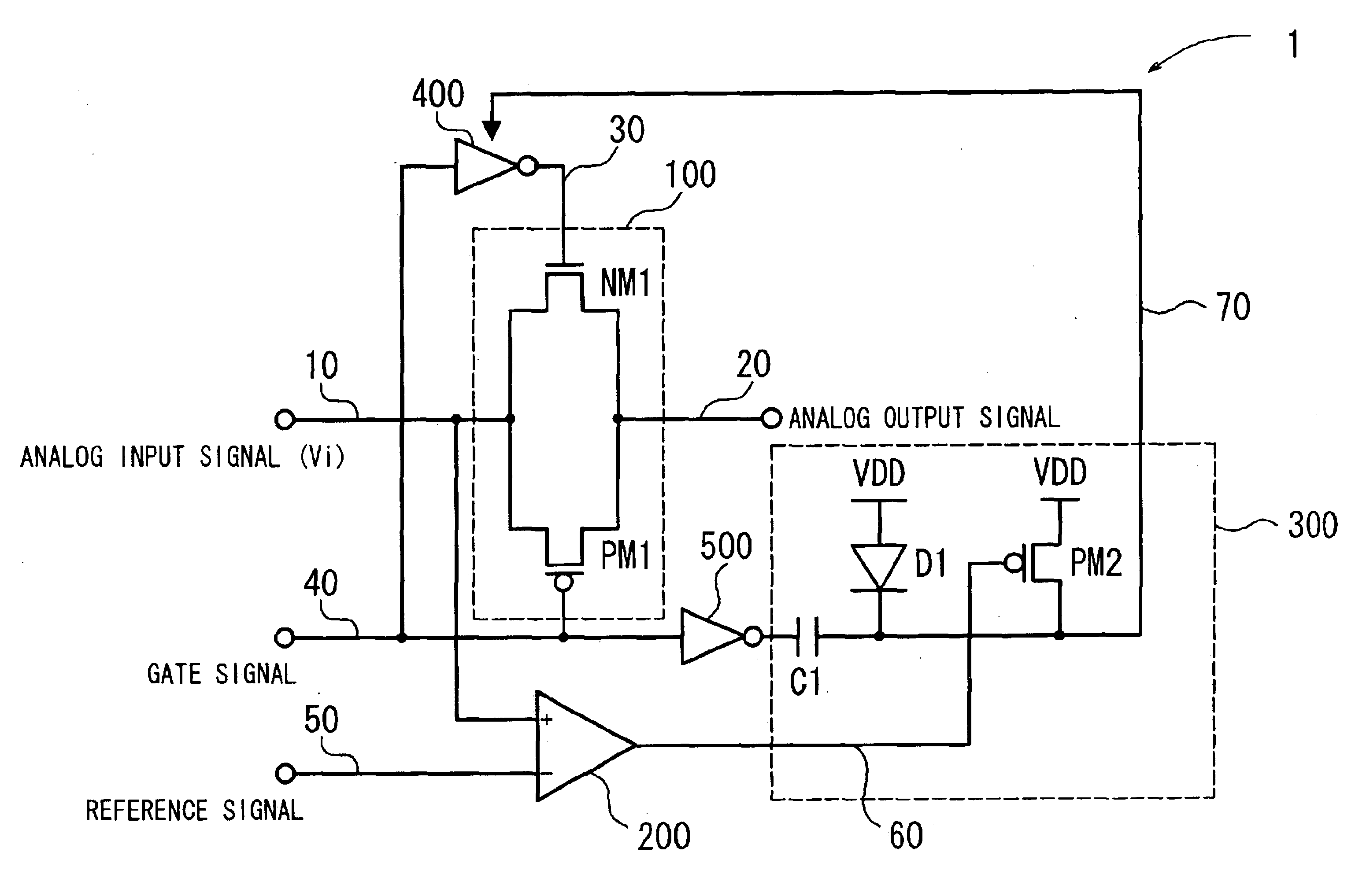
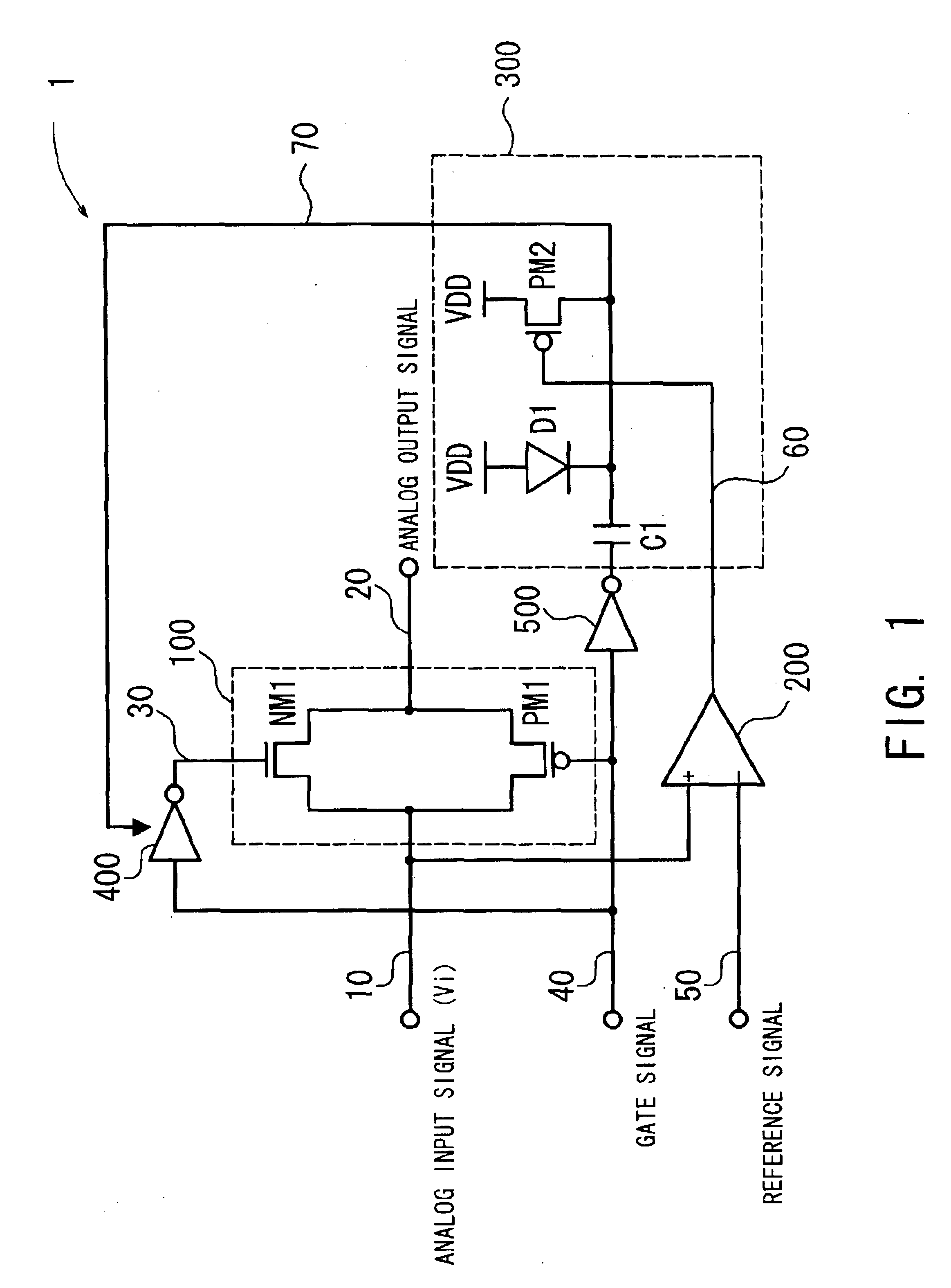
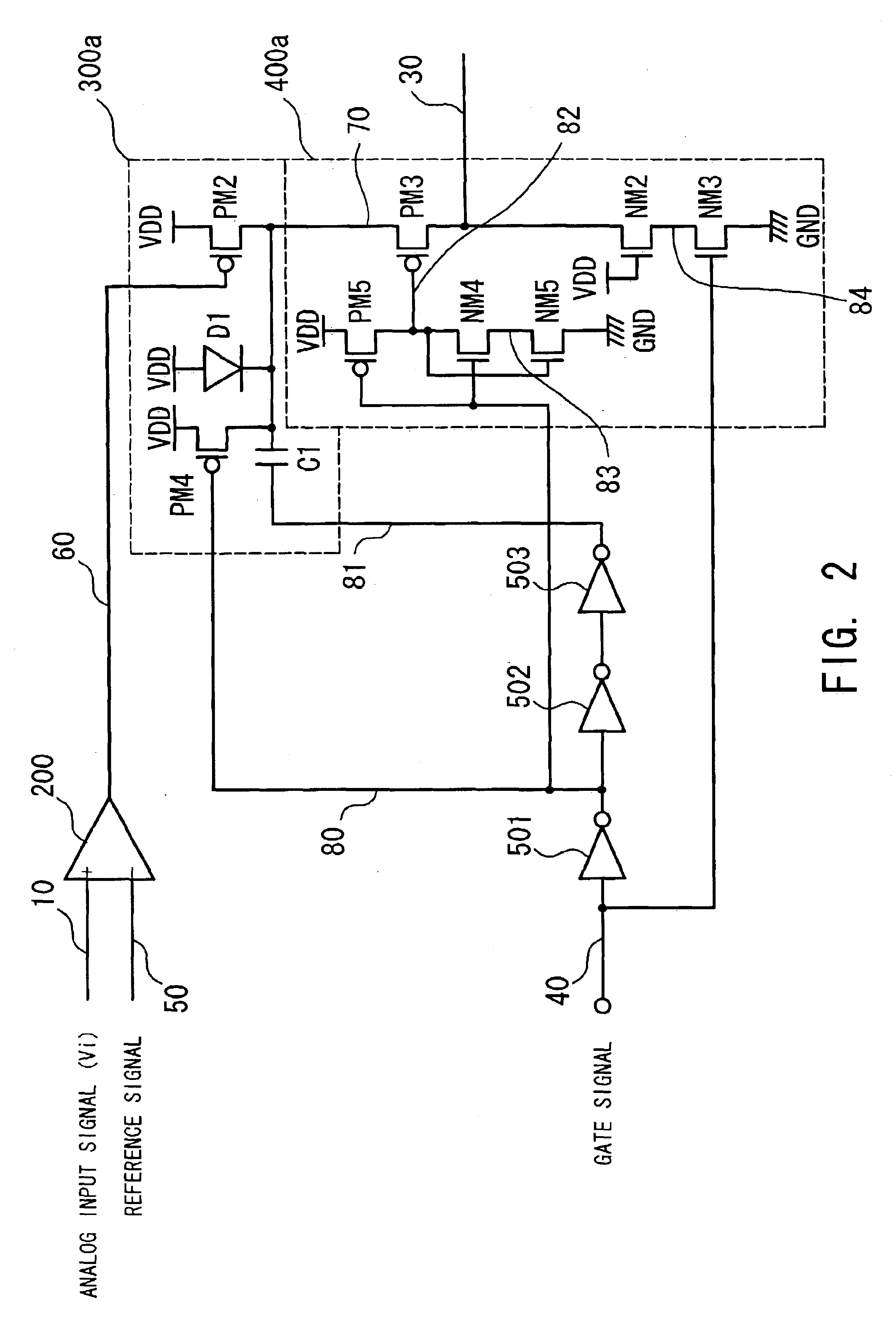
FIG. 1 is a rough circuit diagram of an analog switch circuit according to an embodiment of the present invention.

An analog switch circuit 1 comprises an analog switch section 100 for turning on and off the switch according to a gate signal input and sampling and outputting an analog input signal input, a comparator circuit 200 for comparing the input potential Vi of an analog input signal and the reference potential of a reference signal, a voltage boost circuit 300 for boosting the potential of a gate of an NMOS transistor NM1, a level conversion circuit 400, and an inverter 500 for inverting a gate signal.

A gate signal is, for example, a pulse signal the potential of which changes from the H level to the L level or from the L level to the H level in a predetermined cycle.

The analog switch section 100 includes the NMOS transistor NM1 and a PMOS transistor PM1, to sources of which an analog ...


PUM


Abstract

An analog switch circuit with superior breakdown voltage characteristics that can operate at a high speed at a low power supply voltage. The analog switch circuit includes a comparator circuit for inputting and comparing an analog input signal input to an analog switch section and a reference signal. If the input potential of the analog input signal is lower than the reference potential of the reference signal, a voltage boost circuit sets a potential of a gate of an n MOS transistor included in the analog switch section to a potential of positive power supply voltage. If the input potential of the analog input signal is higher than the reference potential of the reference signal, the voltage boost circuit boosts the potential of the gate to a potential higher than the potential of power supply voltage.

Description

CROSS-REFERENCE TO RELATED APPLICATIONSThis application is based upon and claims the benefits of priority from the prior Japanese Patent Application No. 2002-229123, filed on Aug. 6, 2002, the entire contents of which are incorporated herein by reference.BACKGROUND OF THE INVENTION(1) Field of the InventionThis invention relates to an analog switch circuit for sampling an analog signal and, more particularly, to an analog switch circuit having a voltage boost circuit for boosting the potential of a gate of a MOS field effect-transistor included in an analog switch.(2) Description of the Related ArtSample and hold circuits are important elements in analog-to-digital (A / D) converters which can be fabricated at a comparatively low cost by a complementary metal-oxide semiconductor (CMOS) process. With CMOS large scale integrated circuits (LSIs), usually an analog switch (or a transfer gate) is used for sampling an analog signal.With the progress of microfabrication technologies and the ...

Claims


Application Information

Patent Timeline
Patent Type & Authority Patents(United States)
IPC IPC(8): H03K17/687H03K17/06H03K17/08
CPCH03K17/063H03K17/6872H03K17/6874
Inventor TACHIBANA, SUGURUKATO, TATSUONUNOKAWA, HIDEO
Owner CYPRESS SEMICON CORP
Why Eureka
Try Eureka