Method for etching semiconductor structure and method for forming metal interconnection layer

A metal interconnection layer and semiconductor technology, applied in semiconductor/solid-state device manufacturing, electrical components, circuits, etc., can solve the problems of rough trench line edges, insufficient protection of trench edges, and inability to effectively protect the underlying structure, etc., to achieve Effects of improving line edge roughness and improving breakdown voltage characteristics

Inactive Publication Date: 2010-02-03
SEMICONDUCTOR MANUFACTURING INTERNATIONAL (BEIJING) CORP
View PDF1 Cites 5 Cited by
  • Summary
  • Abstract
  • Description
  • Claims
  • Application Information

AI Technical Summary

Problems solved by technology

[0004] However, since most ArF photoresists do not contain acidic alcohol groups, such photoresists have low affinity to alkaline developing solutions. Glue is more likely to produce the problem of Line Edge Roughness (LER), that is to say, the line edge of the photoresist pattern after exposure and development is jagged and uneven. Therefore, in the etching process, the photolithography The glue cannot effectively protect the underlying structure, and accordingly the edge of the groove formed by etching is also very rough
In addition, as the feature size of semiconductor devices becomes smaller and smaller, the thickness of ArF photoresist is also smaller and smaller. During the etching process, the thinner photoresist layer is over-etched, which is not enough to protect the underlying trench. edge, which will also roughen the edge of the trench line formed by etching
figure 2 It is a top view of the metal interconnect layer in a semiconductor device, such as figure 2 As shown, the grooves for the inlaid metal interconnection layer are etched with the rough-edged ArF photoresist pattern (not shown) as a mask. The light-colored lines in the figure are the line edges of the grooves. It can be seen that the grooves The edge of the line is uneven and rough. This is because the edge of the ArF photoresist layer is rough or thin during the etching process, which causes the edge of the groove under the photoresist layer to be over-etched, which will cause The line width of the metal wiring after forming the metal interconnection layer is uneven, which will seriously affect the breakdown voltage of the semiconductor device
[0005] Similarly, in other semiconductor manufacturing processes that use ArF light sources for lithography, such as the formation of gates and ohmic contacts, etch formation due to rough line edges of ArF photoresists or thin photoresist layers will also occur. The roughness of the line edge of the pattern, which has a bad influence on the reliability of the semiconductor device

Method used


Image

  • Method for etching semiconductor structure and method for forming metal interconnection layer
  • Method for etching semiconductor structure and method for forming metal interconnection layer
  • Method for etching semiconductor structure and method for forming metal interconnection layer

Examples


Embodiment 1

[0060] This example combines the attached Figure 3 to Figure 8 , taking the copper interconnection process as an example, describe in detail the trenches formed by etching the semiconductor structure provided by the present invention for filling the first layer of metal interconnection layer, and describe in detail the metal interconnection provided by the present invention Layer Formation Method Form the first layer of metal interconnection layer.

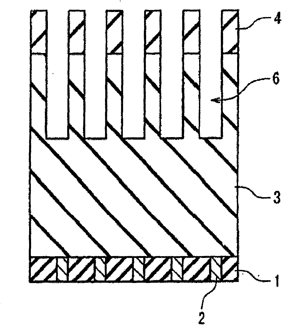
[0061] refer to image 3 As shown, a substrate 100 with a semiconductor device is provided, an active region (not shown) and a metal tungsten plug (not shown) on the active region are provided in the substrate 100, and the metal tungsten plug is used to make the described The active region is electrically connected to the first metal interconnection layer;

[0062] An etch stop layer 105 is formed on the substrate 100 to determine the end point of the etching process and avoid over-etching the tungsten plug in the lower substra...

Embodiment 2

[0080] This embodiment combines the attached Figure 13 to Figure 15 Describe in detail that the gate structure is etched by using the semiconductor structure etching method provided by the technical solution of the present invention.

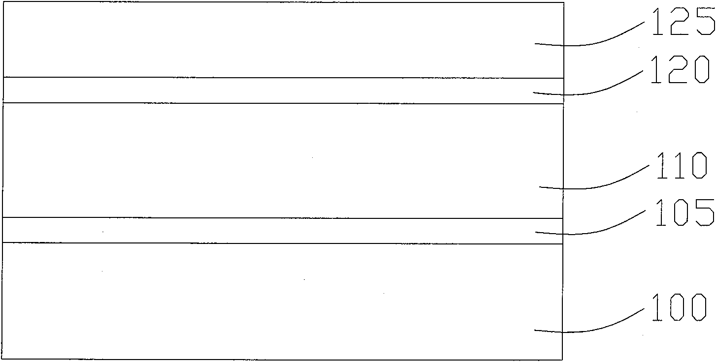
[0081] refer to Figure 13 As shown, a semiconductor substrate 200 having an active region 203 and a shallow trench isolation structure (not shown in the figure) is provided, and a gate dielectric layer 205 is formed on the active region 203. The material of the gate dielectric layer 205 includes but Not limited to silicon oxide, it is prepared by thermal oxidation in an oxidation furnace.

[0082] A gate layer 210 is formed on the gate dielectric layer 205. The material of the gate layer 210 is doped polysilicon. The polysilicon is prepared by low pressure chemical vapor deposition (LPCVD) through silane decomposition reaction, and then doped with polysilicon.

[0083] A bottom anti-reflective coating 215 (Bottom Anti-reflective Coating, BAR...


PUM

PropertyMeasurementUnit
thicknessaaaaaaaaaa

Abstract

The invention provides a method for etching a semiconductor structure and a method for forming a metal interconnection layer. The method for etching the semiconductor structure comprises the steps of:providing a semiconductor substrate, wherein the substrate is provided with a patterned photoresist layer; taking the photoresist layer as a mask to perform plasma etching on the substrate, wherein aplasma etching process at least adopts three fluorocarbon compounds as etching gas; and removing the photoresist layer to form a semiconductor structure. The adoption of the method for etching the semiconductor structure can effectively improve the roughness of line edges of grooves formed by etching. The adoption of the method for forming the metal interconnection layer can effectively improve the roughness of the line edges of the grooves formed by etching, form the metal interconnection layer with straight line edges, and further improve the breakdown voltage characteristics of semiconductor devices.

Description

technical field [0001] The invention relates to the technical field of semiconductor manufacturing, in particular to an etching method for a semiconductor structure and a method for forming a metal interconnection layer. Background technique [0002] With the increasing demand for high integration and high performance of ultra-large-scale integrated circuits, semiconductor technology is developing towards technology nodes with 65nm or even smaller feature sizes, and the wavelength of light sources used for pattern exposure is also getting shorter and shorter. For example, using a 193nm wavelength The ArF laser is used as the light source to expose the key layer pattern of the integrated circuit with a line width below 65nm. Correspondingly, the photoresist material sensitive to the ArF laser (referred to as ArF photoresist) is also widely used in the photolithography process. [0003] The Chinese patent application with publication number CN101131918A provides a method for m...

Claims


Application Information

Patent Timeline
Patent Type & Authority Applications(China)
IPC IPC(8): H01L21/3065H01L21/768H01L21/311
Inventor 赵林林
Owner SEMICONDUCTOR MANUFACTURING INTERNATIONAL (BEIJING) CORP
Why Eureka
Try Eureka