Inertial sensor and preparation method thereof

An inertial sensor and dry etching technology, used in instruments, manufacturing microstructure devices, navigation, etc., can solve problems such as the destruction of the first dielectric layer, and meet the requirements of reducing parasitic capacitance, ensuring device reliability, and lithography accuracy. low effect

Pending Publication Date: 2022-05-17
HANGZHOU SILAN MICROELECTRONICS +1
View PDF0 Cites 0 Cited by
  • Summary
  • Abstract
  • Description
  • Claims
  • Application Information

AI Technical Summary

Problems solved by technology

[0005] Usually by controlling the fumigation rate and fumigation time to ensure that the quality block is movable, the amount of fumigation of the first medium layer is minimized, but it will still cause damage to the first medium layer

Method used


Image

  • Inertial sensor and preparation method thereof
  • Inertial sensor and preparation method thereof
  • Inertial sensor and preparation method thereof

Examples


Embodiment Construction

[0069] Hereinafter, the present invention will be described in more detail with reference to the accompanying drawings. In the various drawings, like elements are indicated with like reference numerals. For the sake of clarity, various parts in the drawings have not been drawn to scale. Also, some well-known parts may not be shown.

[0070] The invention can be embodied in various forms, some examples of which are described below.

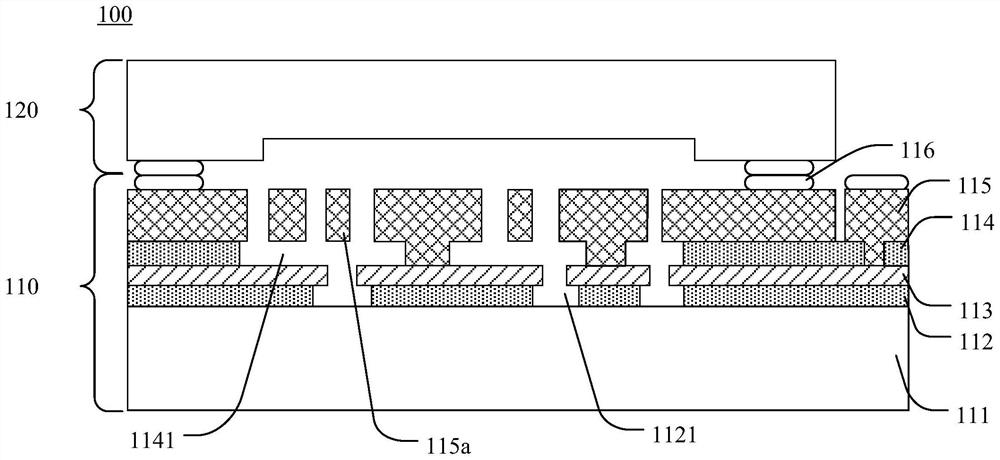
[0071] figure 1 A structural schematic diagram of an inertial sensor in the prior art is shown; as figure 1 As shown, the inertial sensor 100 includes a device chip (Device) 110 and a cap chip (Cap) 120 bonded together. Wherein, the device sheet 110 includes a first substrate 111, a first dielectric layer 112, a first conductive layer 113, a second dielectric layer 114, a second conductive layer 115 and a bonding structure 116 from bottom to top. The cap sheet 120 is bonded to the device sheet 110 through the bonding structure 116 .

[0072] ...


PUM

PropertyMeasurementUnit
thicknessaaaaaaaaaa
thicknessaaaaaaaaaa
thicknessaaaaaaaaaa

Abstract

The invention discloses an inertial sensor and a preparation method thereof. The method comprises the following steps: forming a first dielectric layer and a first conductive layer on a first substrate; forming a first opening in the first conductive layer to expose a part of the surface of the first dielectric layer; forming a protection layer on the first conductive layer, wherein the protection layer covers part of the first conductive layer, the side wall of the first opening and the surface of the first dielectric layer exposed by the first opening; forming a second dielectric layer with a second opening on a part of the first conductive layer and a part of the protective layer; forming a second conductive layer on the second dielectric layer, wherein the second conductive layer fills the second opening; forming a first bonding structure on the second conductive layer; patterning the second conductive layer to form a third opening; removing part of the second dielectric layer through the third opening to form a cavity and a movable mass block; and removing the protective layer exposed on the surfaces of the first conductive layer and the first dielectric layer in the cavity. According to the inertial sensor and the preparation method thereof provided by the embodiment of the invention, the reliability of the inertial sensor is ensured through the protective layer.

Description

technical field [0001] The invention relates to the field of semiconductor technology, in particular to an inertial sensor and a preparation method thereof. Background technique [0002] Surface technology is one of the most common manufacturing processes of micro-electromechanical systems (MEMS). It uses semiconductor substrates as the base and prepares three-dimensional micro-mechanical structures through multiple thin film deposition and pattern processing. [0003] Taking the inertial sensor as an example, the sensor includes a device chip (Device) and a cap chip (Cap) that are bonded together. Wherein, the device sheet includes a first substrate, a first dielectric layer, a first conductive layer, a second dielectric layer, a second conductive layer and a bonding structure from bottom to top. The first conductive layer and the second conductive layer are patterned conductive layers. Among them, the patterned first conductive layer is used as the wiring and the capacit...

Claims


Application Information

Patent Timeline
Patent Type & Authority Applications(China)
IPC IPC(8): B81C1/00G01C21/16
CPCB81C1/00349B81C1/00531B81C1/00095G01C21/166
Inventor 汪建平季锋
Owner HANGZHOU SILAN MICROELECTRONICS
Why Eureka
Try Eureka