Nitride semiconductor substrate

Active Publication Date: 2017-01-12
COORSTEK INC
View PDF1 Cites 5 Cited by
  • Summary
  • Abstract
  • Description
  • Claims
  • Application Information

AI Technical Summary

Benefits of technology

[0014]According to the present invention, the initial layer including the base substrate and the initial nitride thereon includes the recesses, each of which has a diameter of 6 nm or more and 60 nm or less

Problems solved by technology

If the uniform growth of the nitride semiconductor layer on the entire surface of the substrate is failed, the high-quality nitride semiconductor layer may not be obtained.
However, forming the unevenness of such a size within the surface of the substrate with high accuracy results in the cost increase of the base substrate.
Mo

Method used


Image

  • Nitride semiconductor substrate
  • Nitride semiconductor substrate
  • Nitride semiconductor substrate

Examples


example 1

(Preparation of Base Substrate)

[0063]First, a silicon single-crystal substrate doped with boron and having a diameter of 6 inches, a plane orientation of (111), a specific resistance of 0.004 Ωcm, and an oxygen concentration of 1.0×10¹⁸ atoms / cm3 was prepared as the base substrate.

(Stacking Initial Nitride and Nitride Semiconductor)

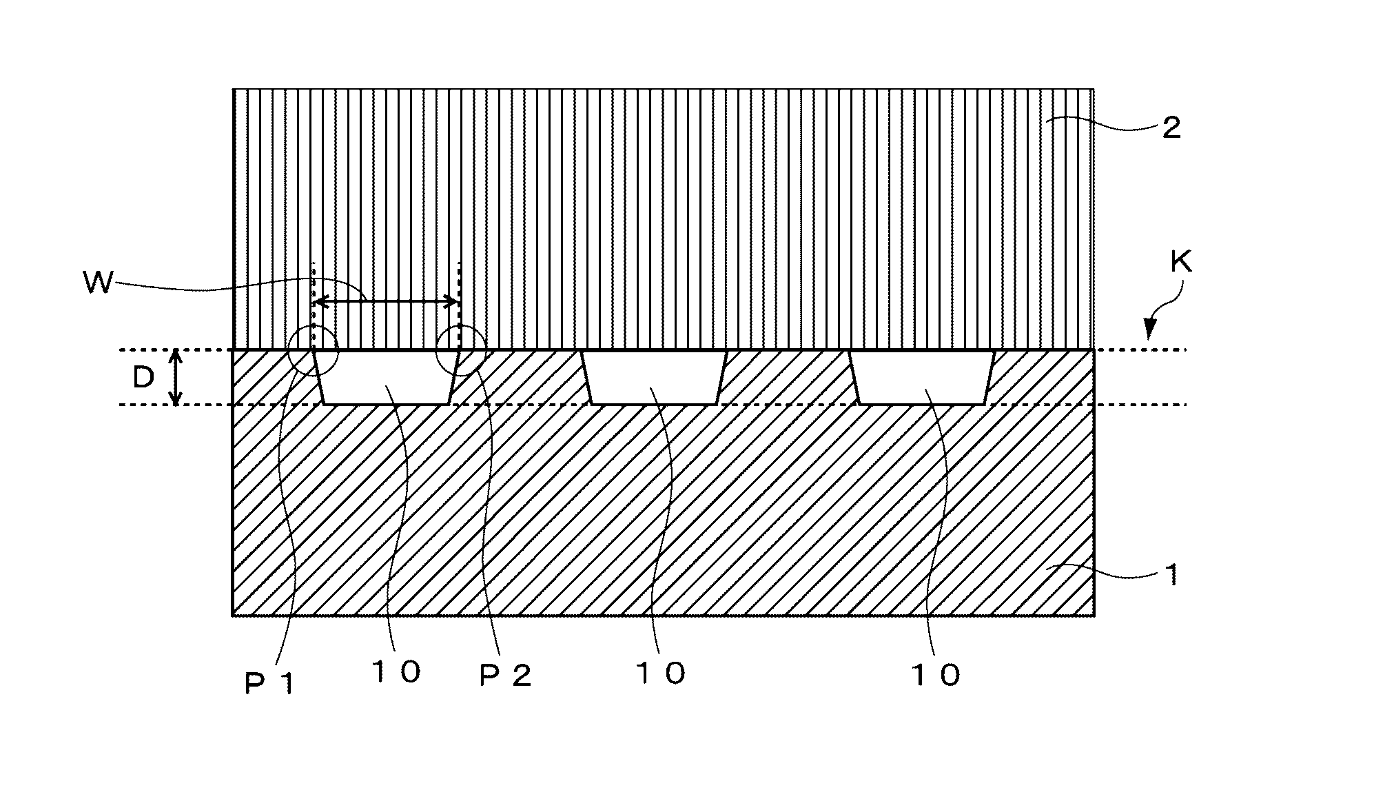
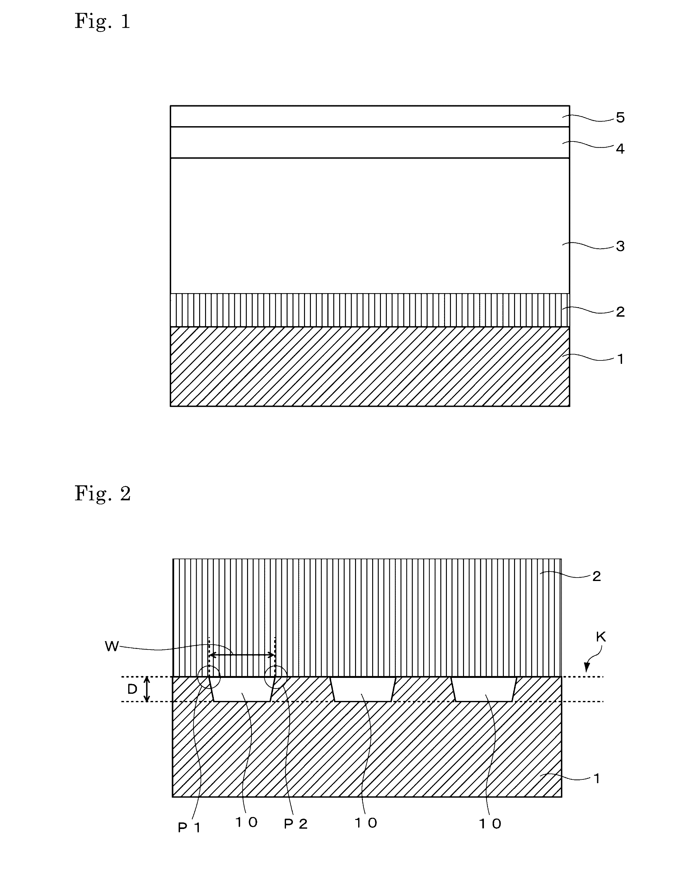
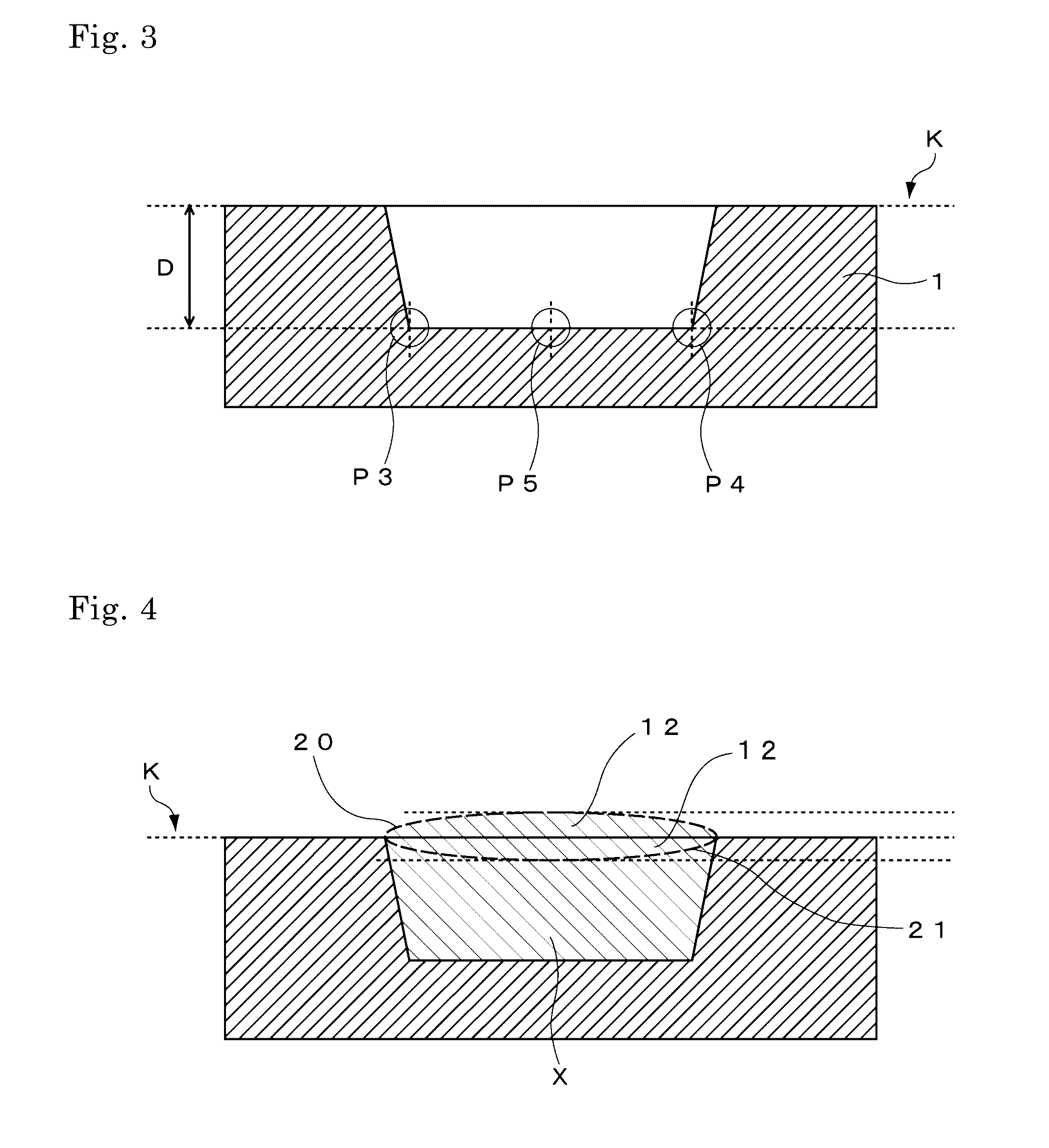
[0064]The nitride semiconductor substrate with the layer structure as illustrated in FIG. 1 was manufactured through the following process.

[0065]First, the silicon single-crystal substrate was set in the MOCVD apparatus, and the temperature was increased and the gas was replaced. After that, the thermal treatment was performed for 1000° C.×15 minutes in the 100% hydrogen atmosphere.

[0066]Subsequently, the layer 2 of the initial nitride including AlN single crystal with a carbon concentration of 1×10¹⁸ atoms / cm3 and a thickness of 100 nm was grown in the vapor phase at 500° C. using trimethyl aluminum (TMA) and ammonia (NH3) as the source gas. Note that in...

example 2

[0078]A sample according to Example 2 was manufactured and evaluated in a manner similar to Example 1 except that the condition of the thermal treatment was set to 1000° C.×7 minutes.

example 3

[0079]A sample according to Example 3 was manufactured and evaluated in a manner similar to Example 1 except that the condition of the thermal treatment was set to 1000° C.×10 minutes.


PUM


Abstract

The present invention provides a nitride semiconductor substrate having an initial nitride and a nitride semiconductor sequentially stacked on one principal plane of a base substrate, wherein the nitride semiconductor substrate comprises recesses depressed from an interface between the base substrate and the initial nitride toward the base substrate along one arbitrary cross section; the recesses each have a diameter of 6 nm or more and 60 nm or less and are formed at a density of 3×10⁸ pieces/cm2 or more and 1×10¹¹ pieces/cm2 or less; and the recess preferably has a depth of 3 nm or more and 45 nm or less from the interface between the base substrate and the initial nitride toward the base substrate.

Description

BACKGROUND OF THE INVENTION[0001]Field of the Invention[0002]The present invention relates to a nitride semiconductor substrate suitably used for the power semiconductor, electronic devices, etc.[0003]Description of the Related Art[0004]As the technique of providing the crystal growth method for a nitride semiconductor for improving the performance and the lifetime of the semiconductor device by reducing the dislocation density, JP-A-2002-323733 has disclosed the crystal growth method for a nitride semiconductor, the method including a first crystal growth step of forming a plurality of island-shaped crystal regions of nitride semiconductor on a base through vapor-phase growth, and a second crystal growth step of growing the island-shaped crystal regions further while linking the borders of the island-shaped crystal regions. In this method, the crystal growth speed in the second crystal growth step is set higher than the crystal growth speed in the first crystal growth step, or the ...

Claims


Application Information

Patent Timeline
IPC IPC(8): H01L21/02H01L29/20
CPCH01L21/02694H01L21/0243H01L29/2003H01L21/0254H01L21/02458H01L21/02381H01L21/02433H01L21/0262H01L21/02639H01L29/7786H01L29/0661H01L29/34
Inventor OMORI, NORIKOOISHI, HIROSHIABE, YOSHIHISAKOMIYAMA, JUNERIGUCHI, KENICHIWATANABE, TOMOKO
Owner COORSTEK INC
Why Eureka
Try Eureka