

CMOS imager having a nitride dielectric
a dielectric and cmos imager technology, applied in semiconductor devices, diodes, electrical devices, etc., can solve the problems of high power dissipation of large arrays, ccd imagers also suffer from a number, and are susceptible to radiation damage, so as to improve the breakdown voltage and breakdown voltage characteristics, the effect of increasing the capacitan
- Summary
- Abstract
- Description
- Claims
- Application Information
AI Technical Summary
Benefits of technology
Problems solved by technology
Method used
Image

Examples
Embodiment Construction
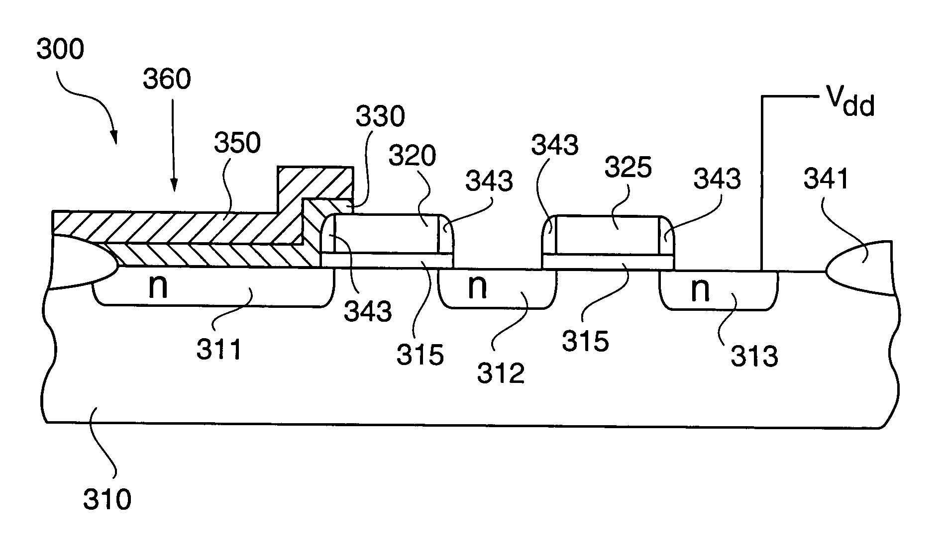
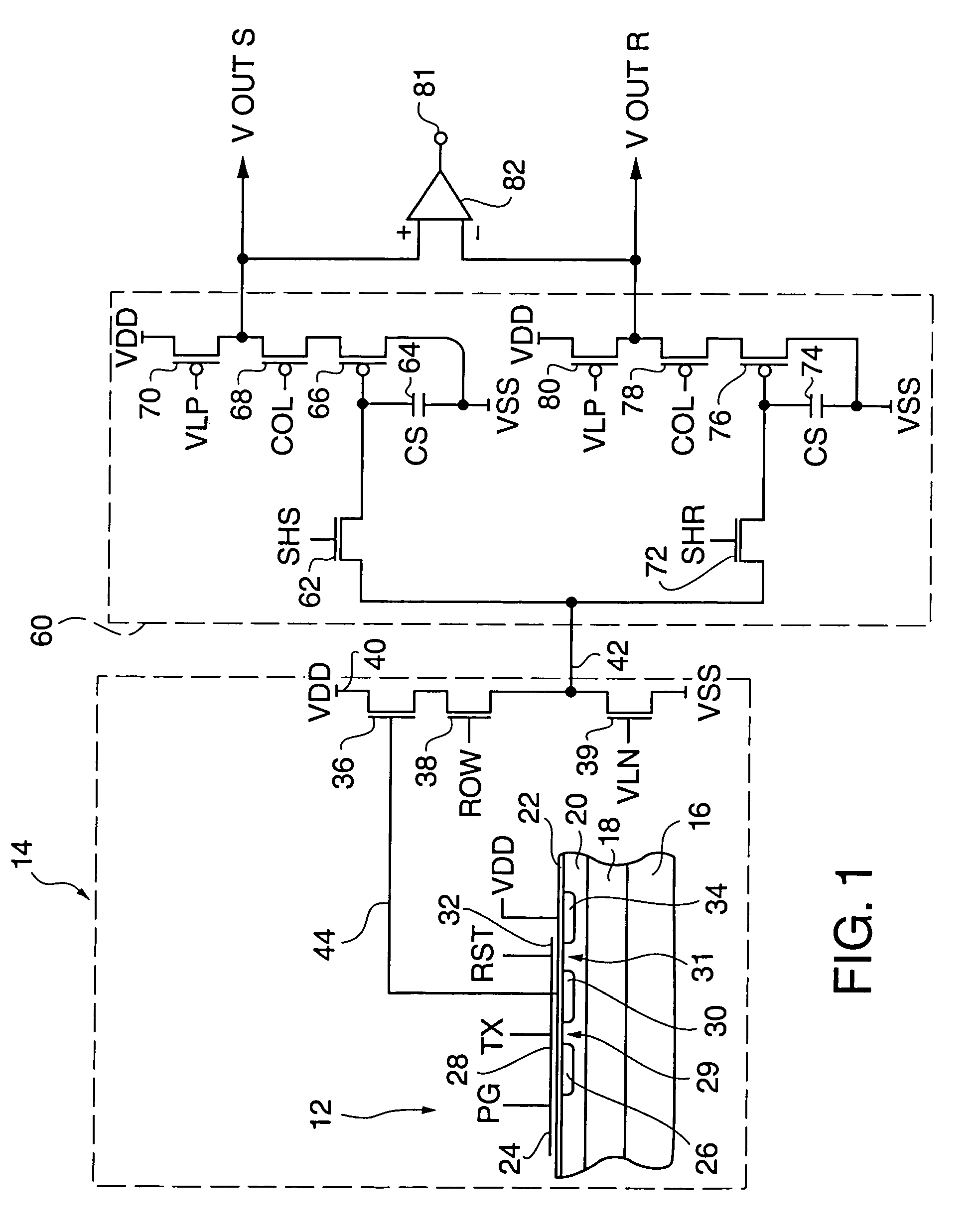
[0033]The present invention will now be described with reference to the figures. While the invention is described with respect to an imager pixel using n-channel transistors in a p-well, it should be understood that the present invention may also be used with p-channel transistors in an n-well. Referring now to FIG. 4. This figure shows a portion of a CMOS imager 300 at one point in the fabrication process. The substrate 310 has field oxide regions 341 formed to surround and isolate the cells which may be formed by thermal oxidation.
[0034]A first insulating layer 315 is grown over a surface of substrate 310. Preferably the first insulating layer 315 is a silicon dioxide layer which may be formed, i.e., grown, by conventional methods. Preferably the first insulating layer 315 is grown by thermal oxidation of silicon and the first insulating layer 315 has a thickness of from about 30 to about 500 angstroms. A transfer gate stack 320 and a reset gate stack 325 are deposited and pattern...
PUM
 Abstract
Description
Claims
Application Information