Method for manufacturing flexible touch control display screen

a touch control display and display screen technology, applied in the field of display panels, can solve the problems of inability to achieve lcds, users are getting increasingly unsatisfied with the resolution of displayed images, and the production of oled displays with high quality and high resolution still faces a lot of challenges, so as to reduce the number of masks used, simplify the manufacturing process, and reduce manufacturing costs

Active Publication Date: 2019-05-30
WUHAN CHINA STAR OPTOELECTRONICS SEMICON DISPLAY TECH CO LTD
View PDF0 Cites 11 Cited by
  • Summary
  • Abstract
  • Description
  • Claims
  • Application Information

AI Technical Summary

Benefits of technology

[0058]Compared to conventional techniques, the present disclosure is characterized by patterning the first photoresist layer with use of a multi-transmittance mask, so that a first contact hole and a second contact hole having different depths are formed in the insulation layer. The present disclosure reduces number of masks used in the manufacturing process and simplifies the manufacturing process, lowering manufacturing cost and improving manufacturing efficiency. Furthermore, since a first insulation layer is formed to block oxygen and water from eroding the OLED display layer, the first insulation layer has the functional effect of protecting the OLED display layer.

Problems solved by technology

In comparing OLED displays with LCDs, OLED displays save more energy, are thinner, and have wider viewing angles, which the LCDs cannot achieve.
Nevertheless, users are getting increasingly unsatisfied with the resolution of displayed images, and production of OLED displays with high quality and high resolution still faces a lot of challenges.
However, conventional touch control screens manufactured, based on a transparent conductive film, cannot meet desired flexibility requirements.
On one other hand, because the conventional touch control screens have to be first manufactured independently, and then adhered to upper surfaces of the OLED screens via an optical transparent adhesive to form a complete touch control display module, such technology requires an additional bonding step and increases the entire thickness of the module.
This is not helpful in enabling flexible touch control display screens being light weight and thin.
This not only increases manufacturing cost but lowers manufacturing efficiency.

Method used


Image

  • Method for manufacturing flexible touch control display screen
  • Method for manufacturing flexible touch control display screen
  • Method for manufacturing flexible touch control display screen

Examples


Embodiment Construction

[0062]The following embodiments refer to the accompanying drawings for exemplifying specific implementable embodiments of the present disclosure. Moreover, directional terms described by the present disclosure, such as upper, lower, front, back, left, right, inner, outer, side, etc., are only directions by referring to the accompanying drawings, and thus the used directional terms are used to describe and understand the present disclosure, but the present disclosure is not limited thereto. In the drawings, the same reference symbol represents the same or similar components.

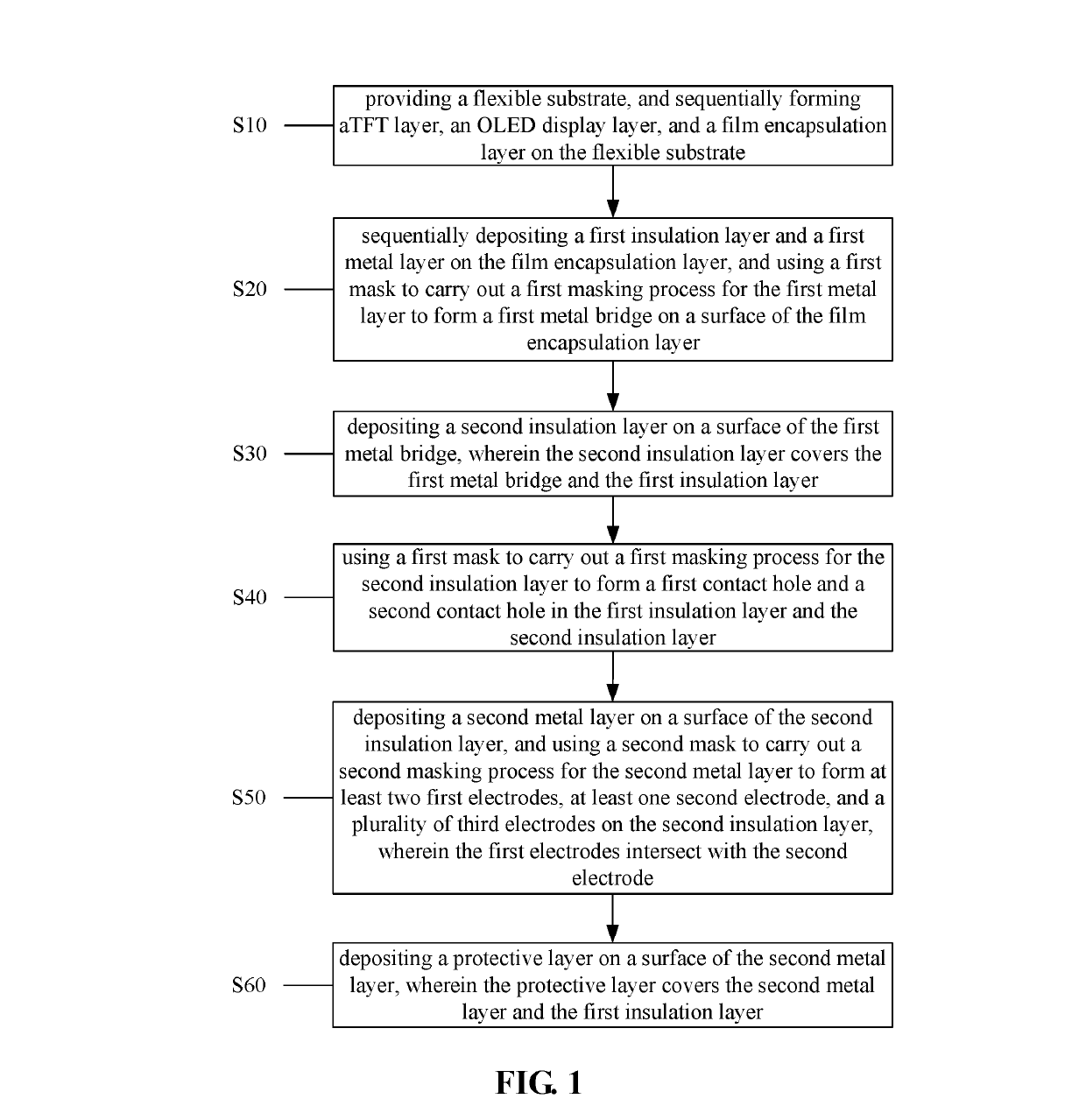
[0063]FIG. 1 is a flowchart showing a method for manufacturing a flexible touch control display screen according to one preferred embodiment of the present disclosure. The method includes the following steps.

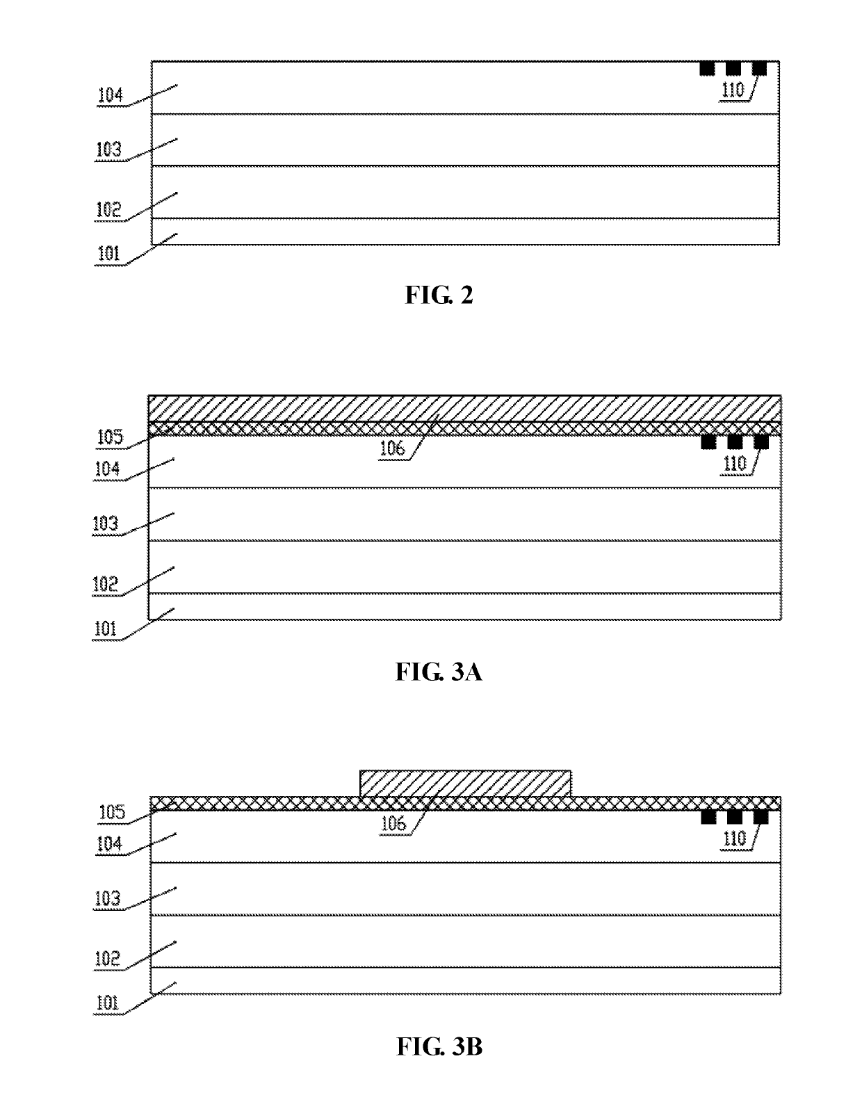
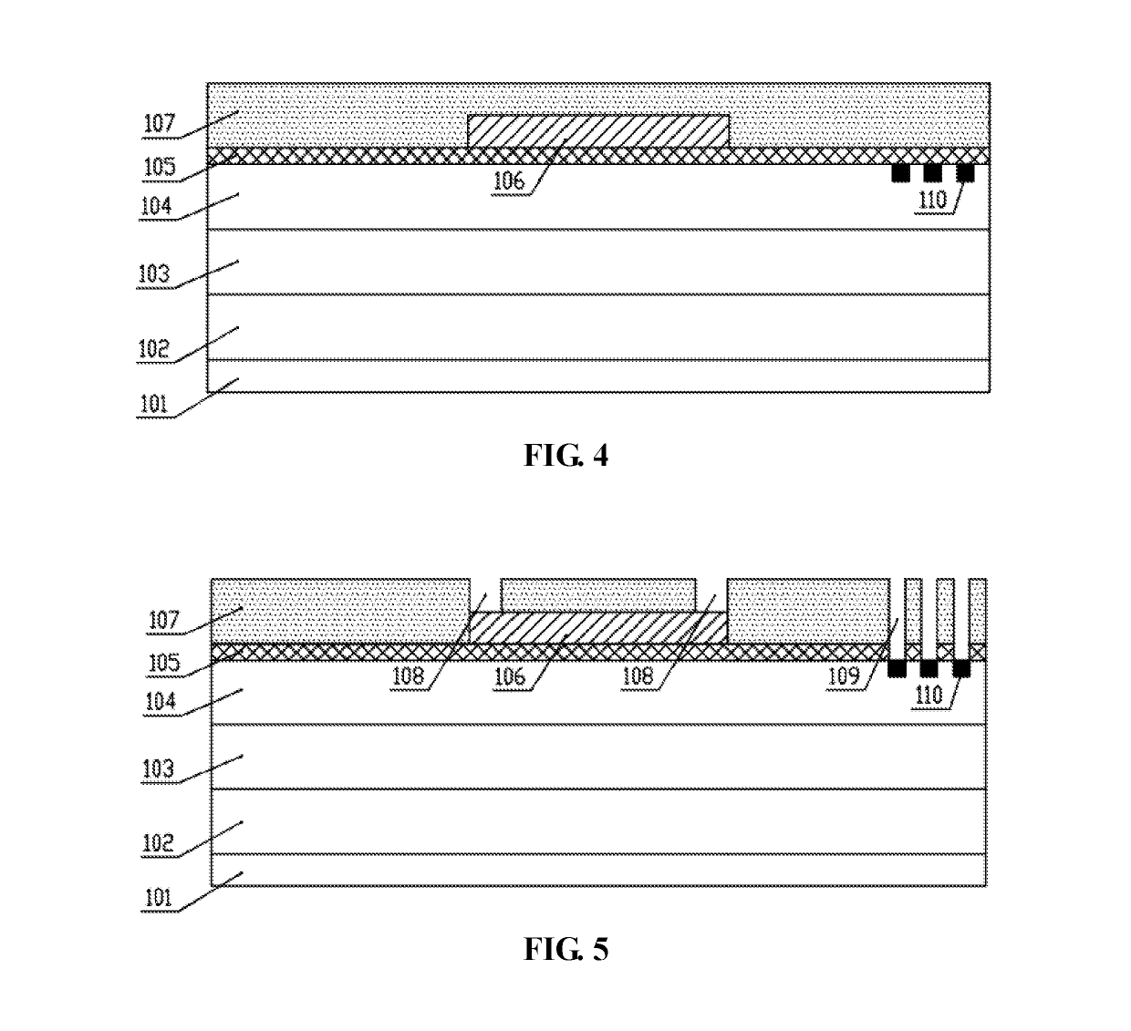
[0064]In a step S10, a flexible substrate 101 is provided, and a thin film transistor (TFT) layer 102, an organic light-emitting diode (OLED) display layer 103, and a film encapsulation layer 104 are sequentia...


PUM


Abstract

The present disclosure provides a method for manufacturing a flexible touch control display screen. A TFT layer, an OLED display layer, and a film encapsulation layer are sequentially formed on the substrate. A first insulation layer, a first metal bridge, a second insulation layer, a second metal layer, and a protective layer are sequentially formed on the film encapsulation layer. By patterning the first photoresist layer with the use of a multi-transmittance mask, a first contact hole and a second contact hole having different depths are formed in the insulation layer.

Description

FIELD OF INVENTION[0001]The present disclosure relates to the field of display panels, and more particularly to a method for manufacturing a flexible touch control display screen.BACKGROUND[0002]Among various types of flat panels, organic light-emitting diode (OLED) displays have outstanding properties, including being light weight, thin, self-illuminating, having a short response time, wide viewing angles, a wide color gamut, high brightness, and low power consumption. Thus, OLED displays have gradually become a mainstream, next generation display technology. In comparing OLED displays with LCDs, OLED displays save more energy, are thinner, and have wider viewing angles, which the LCDs cannot achieve. Nevertheless, users are getting increasingly unsatisfied with the resolution of displayed images, and production of OLED displays with high quality and high resolution still faces a lot of challenges.[0003]Current touch control technology can be generally classified to include an out-...

Claims


Application Information

Patent Timeline
Patent Type & Authority Applications(United States)
IPC IPC(8): H01L51/56H01L51/00H01L51/52H01L27/32G06F3/044G06F3/041
CPCH01L51/56H01L51/0097H01L51/5253H01L27/323H01L27/3244G06F3/044G06F3/0412H01L2251/5338H01L2227/323G06F2203/04103G06F2203/04102G06F2203/04111H10K59/40H10K50/844H10K71/00G06F3/0446G06F3/0444H10K77/111H10K2102/311H10K59/12H10K59/1201
Inventor YE, JIAN
Owner WUHAN CHINA STAR OPTOELECTRONICS SEMICON DISPLAY TECH CO LTD
Why Eureka
Try Eureka