Supercharge Your Innovation With Domain-Expert AI Agents!

Align the imaging device

An imaging device and imaging technology, applied in the semiconductor field, can solve the problems of low energy utilization rate and uneconomical, etc., and achieve the effect of simple and convenient switching

Active Publication Date: 2017-01-25
SHANGHAI MICRO ELECTRONICS EQUIP (GRP) CO LTD
View PDF9 Cites 0 Cited by
  • Summary
  • Abstract
  • Description
  • Claims
  • Application Information

AI Technical Summary

Problems solved by technology

Even if the lighting mode is changed on this basis to achieve the purpose of image enhancement, it can only be done by changing the shape and size of the aperture, which is a very low energy utilization and uneconomical way

Method used


Image

  • Align the imaging device
  • Align the imaging device
  • Align the imaging device

Examples


Embodiment 1

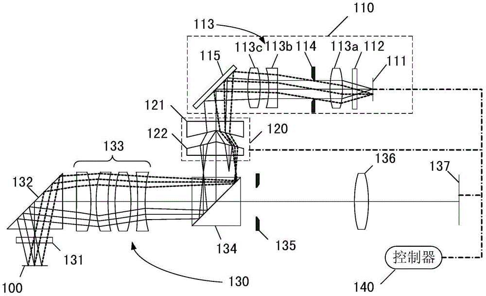
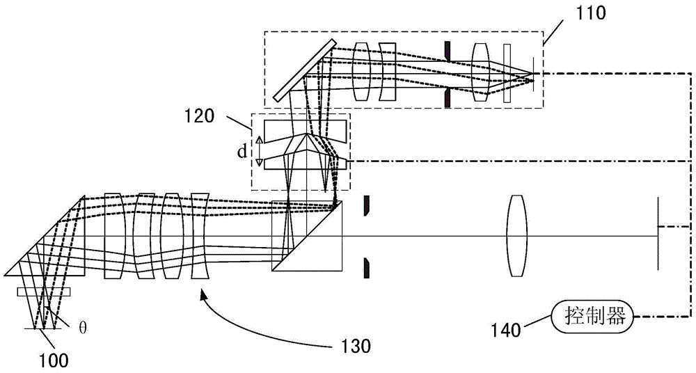
[0030] Such as figure 1 As shown, in this embodiment, the alignment forming device is composed of two parts: an alignment imaging lens and a controller 140, wherein the alignment imaging lens is used to image the alignment marks on the surface of the silicon wafer 100, and the imaging assembly 130 It consists of two parts, coaxial lighting components.

[0031] The coaxial lighting assembly includes a lighting front group 110 and a corner cube prism group 120 , and the main function of the coaxial lighting assembly is to provide different lighting modes for aligning the imaging lens to enhance the image. Wherein, the illumination front group 110 is used to provide illumination beams, which sequentially include: a light source 111, a filter assembly 112, an illumination lens group 113, an illumination field diaphragm 114, and a reflection unit 115 along the direction of light propagation; further, The illumination lens group 113 includes: first, second and third illumination le...

Embodiment 2

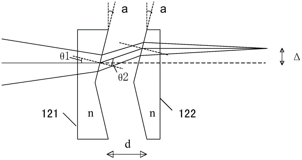
[0051] The difference between this embodiment and Embodiment 1 is that the present embodiment transforms the corner cube group into a Fresnel lens or a binary optical element 120' equivalently, and its equivalent schematic diagram is as follows Figure 8a and Figure 8b shown.

[0052] The switching mode of the different illumination modes of the Fresnel lens or the binary optical element 120' is the same as that of the corner cube prism group, and the partial schematic diagram of the switching of the illumination modes is as follows Figures 9a-9c As shown, the binary optical element adopts a binary optical corner cube. Since the other parts and work flow of the alignment forming device in this embodiment are the same as those in Embodiment 1, details are not repeated here.

[0053] In summary, the alignment imaging device of the present invention includes: an imaging component, a coaxial lighting component, and a controller; wherein, the coaxial lighting component includes...


PUM


Abstract

The invention discloses an alignment imaging device which comprises a coaxial lighting assembly, an imaging assembly and a controller, wherein the coaxial lighting assembly comprises a lighting front group and an image enhancement assembly, and a cube-corner prism group, a Fresnel lens or a binary optical element is adopted as the image enhancement assembly; the imaging assembly sequentially comprises an imaging front group, a light splitting unit, an imaging aperture diaphragm, an imaging rear group and a detector along the light propagation direction; the controller is connected with the lighting front group, the image enhancement assembly and the detector; the light beam generated by the lighting front group is adjusted by the image enhancement assembly and is then irradiated onto a silicon slice by the light splitting unit and the imaging front group; an alignment mark on the silicon slice is imaged onto the detector by the imaging front group, the light splitting unit, the imaging aperture diaphragm and the imaging rear group. Compared with the prior art, the cube-corner prism group, the Fresnel lens or the binary optical element is adopted for the alignment imaging device to form a Kohler coaxial illumination light path together with the lighting front group and the imaging front group, so that different image enhancement modes can be rapidly, simply and conveniently switched by being aligned to an imaging lens; in the switching process, extra energy loss is not caused.

Description

technical field [0001] The invention relates to the technical field of semiconductors, in particular to an alignment and imaging device in semiconductor photolithography equipment. Background technique [0002] Microelectronics technology plays an important role in the information industry revolution, and lithography machine is an indispensable tool in the manufacturing of microelectronic devices. The alignment subsystem is one of the key components in lithography machine. The overlay accuracy is closely related. With the increase of the types of semiconductor devices, the process conditions that the alignment subsystem needs to deal with are becoming more and more complicated. This situation is especially obvious for the back-end packaging lithography machine, so higher requirements are put forward for the performance of the alignment subsystem. Require. [0003] For a system that uses the principle of visual sensing system (MVS) for alignment, the imaging quality of the ...

Claims


Application Information

Patent Timeline
Patent Type & Authority Patents(China)
IPC IPC(8): G03F7/20G02B27/00
Inventor 于大维潘炼东
Owner SHANGHAI MICRO ELECTRONICS EQUIP (GRP) CO LTD
Features
  • R&D
  • Intellectual Property
  • Life Sciences
  • Materials
  • Tech Scout
  • Unparalleled Data Quality
  • Higher Quality Content
  • 60% Fewer Hallucinations
Learn More