Optimization method for local layout of FPGA chips

An optimization method and layout technology, applied in special data processing applications, instruments, electrical digital data processing, etc., can solve problems such as no good solutions have been proposed, and achieve the effect of realizing FPGA layout and taking into account efficiency

Active Publication Date: 2015-06-10
CAPITAL MICROELECTRONICS
View PDF2 Cites 6 Cited by
  • Summary
  • Abstract
  • Description
  • Claims
  • Application Information

AI Technical Summary

Problems solved by technology

In this regard, the industry has not yet proposed a good solution

Method used


Image

  • Optimization method for local layout of FPGA chips
  • Optimization method for local layout of FPGA chips
  • Optimization method for local layout of FPGA chips

Examples


Embodiment Construction

[0035] The technical solutions of the present invention will be described in further detail below with reference to the accompanying drawings and embodiments.

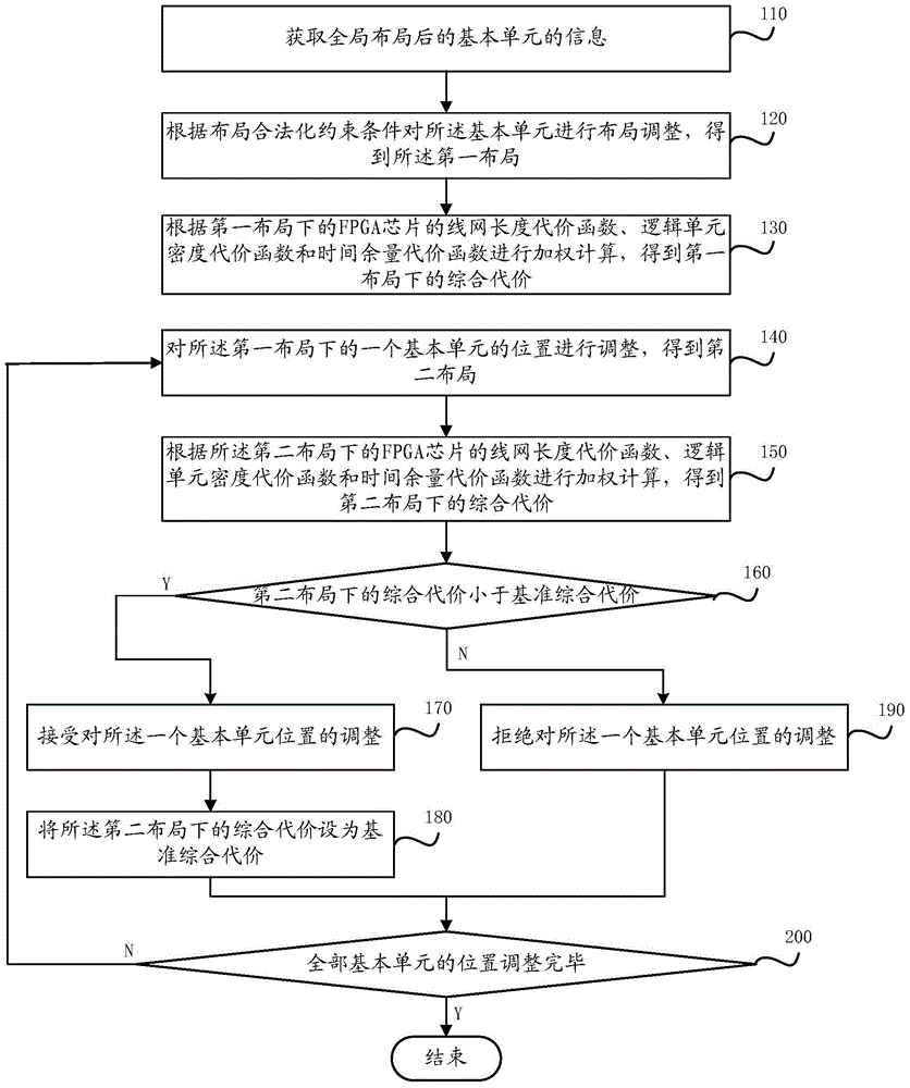
[0036] figure 1 It is a flowchart of a method for optimizing a local layout of an FPGA chip provided by an embodiment of the present invention. As shown in the figure, the method includes the following steps:

[0037] Step 110, obtaining the information of the basic unit after the global layout;

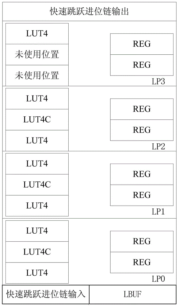
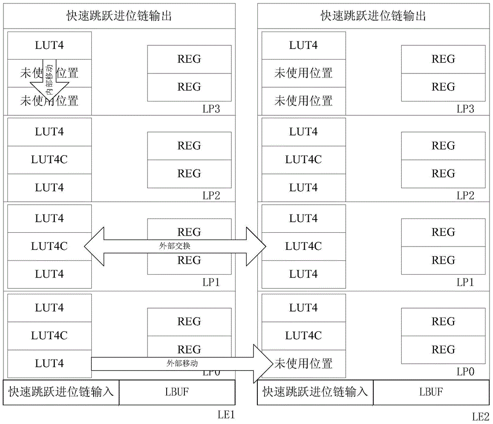
[0038] Specifically, according to the user design, circuit synthesis and library mapping are performed on the user design to obtain the basic unit of the global layout. In an example, the basic unit may include three basic forms: a four-input look-up table (LUT4, LUT4C) and a register (REG), a separate four-input look-up table, and a separate register.

[0039] After the global layout, the lookup tables and registers between the logic elements (Logic Elements, LEs) inside the FPGA chip and within the logic elements are all...


PUM


Abstract

The invention relates to an optimization method for local layout of FPGA chips. The method comprises the following steps: carrying out weighting calculation according to the wire network length cost function, logical unit density cost function and time margin cost function of the FPGA chips under a first layout to obtain comprehensive cost under the first layout; setting the comprehensive cost under the first layout to be reference comprehensive cost; adjusting the position of a basic unit under the first layout to obtain a second layout; carrying out weighting calculation according to the wire network length cost function, logical unit density cost function and time margin cost function of the FPGA chips under the second layout to obtain comprehensive cost under the second layout; when the comprehensive cost under the second layout is smaller than the reference comprehensive cost, receiving the adjustment for the position of one basic unit; setting the comprehensive cost under the second layout to be the reference comprehensive cost; adjusting the position of the next basic unit under the first layout.

Description

technical field [0001] The invention relates to the technical field of integrated circuit design in the field of microelectronics, in particular to a method for optimizing the local layout of Field Programmable Gate Array (Field Programmable Gate Array, FPGA) chips. Background technique [0002] FPGA is a logic device with abundant hardware resources, powerful parallel processing capability and flexible reconfigurable capability. These features make FPGA more and more widely used in data processing, communication, network and many other fields. [0003] With the expansion of FPGA chip scale, chip layout becomes more and more critical and important, which directly determines the complexity and success rate of chip wiring, and affects the chip area, frequency and other performance. Therefore, it is necessary to comprehensively consider the cost of various aspects in the chip layout. Under the condition of satisfying various constraints, how to ensure the area, frequency and d...

Claims


Application Information

Patent Timeline
Patent Type & Authority Applications(China)
IPC IPC(8): G06F17/50
Inventor 蒋中华虞健吴鑫刘明
Owner CAPITAL MICROELECTRONICS
Why Eureka
Try Eureka