Display device, array substrate and manufacturing method thereof

A technology of an array substrate and a manufacturing method, which is applied in the field of display devices, can solve the problems of easy electrostatic breakdown of circuits and poor anti-static effect, etc.

Active Publication Date: 2018-02-02
BOE TECH GRP CO LTD +1
View PDF7 Cites 0 Cited by
  • Summary
  • Abstract
  • Description
  • Claims
  • Application Information

AI Technical Summary

Problems solved by technology

[0008] The purpose of the present invention is to provide a display device, an array substrate and a manufacturing method thereof, so as to overcome the defects that the array substrate circuit in the prior art is easily broken down by static electricity and has poor antistatic effect

Method used


Image

  • Display device, array substrate and manufacturing method thereof
  • Display device, array substrate and manufacturing method thereof
  • Display device, array substrate and manufacturing method thereof

Examples


Embodiment Construction

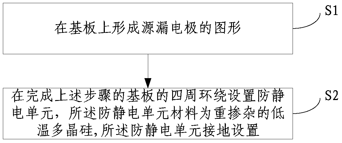
[0030] The specific implementation manners of the present invention will be further described in detail below in conjunction with the accompanying drawings and embodiments. The following examples are used to illustrate the present invention, but are not intended to limit the scope of the present invention.

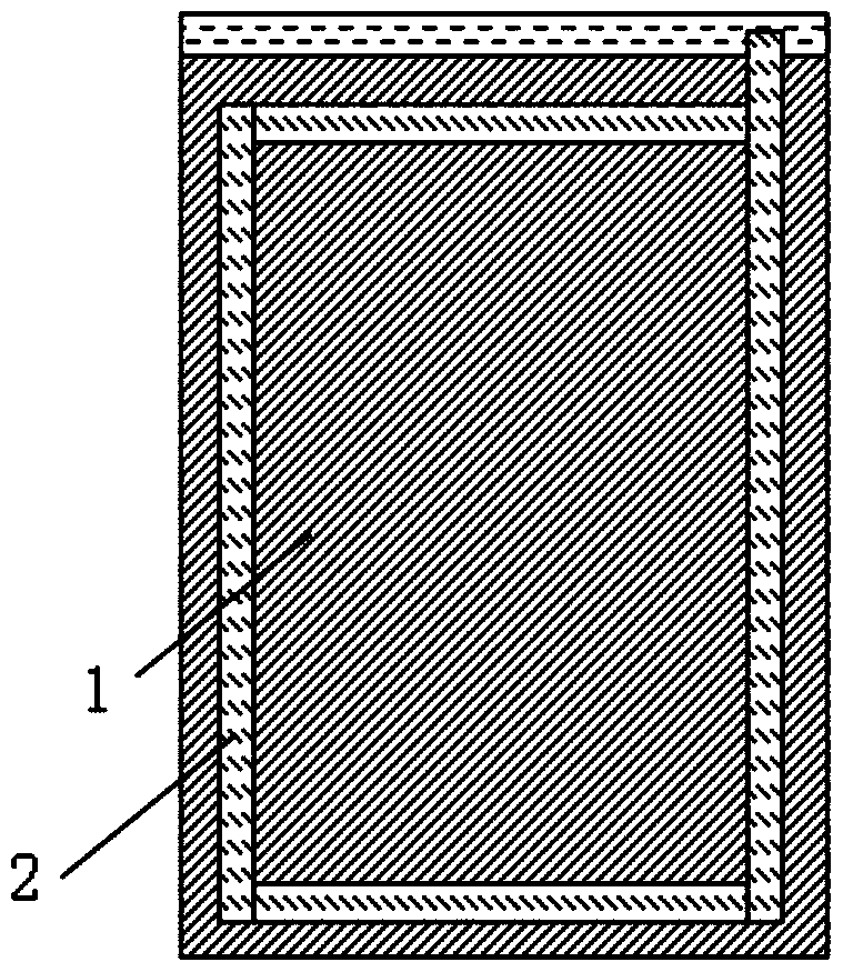
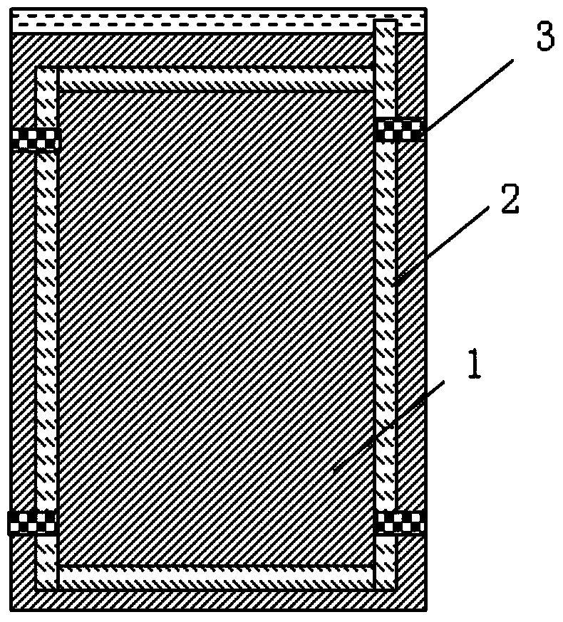
[0031] Such as figure 1 As shown, the present invention provides an array substrate, including a substrate 1 and a source-drain electrode layer on the substrate. The source-drain electrode layer is made of a low-resistance material, such as aluminum or titanium.

[0032] The substrate 1 is surrounded by an anti-static unit 2, and the material of the anti-static unit is heavily doped low-temperature polysilicon; the anti-static unit is grounded.

[0033] Using heavily doped low-temperature polysilicon as the antistatic unit 2, because the heavily doped low-temperature polysilicon has both a certain resistance and conductivity, it can play the role of attracting current, co...


PUM


Abstract

The present invention relates to the field of display technology, and in particular, to a display device, an array substrate and a manufacturing method thereof. The display device includes a substrate and a source-drain electrode layer on the substrate, the source-drain electrode layer is made of a low-resistance material; an anti-static unit is arranged around the substrate, and the anti-static unit material is heavily doped low-temperature polysilicon , the anti-static unit is grounded. In the display device, the array substrate and the manufacturing method thereof provided by the present invention, an anti-static unit made of heavily doped low temperature polysilicon is arranged around the substrate, since the heavily doped low temperature polysilicon has both a certain resistance performance and electrical conductivity The performance can play the role of attracting current, consuming current, and conducting current, ensuring the circuit safety of the array substrate to the greatest extent, and improving the quality of the final product.

Description

technical field [0001] The present invention relates to the field of display technology, in particular to a display device, an array substrate and a manufacturing method thereof. Background technique [0002] Low Temperature Poly-silicon Thin Film Transistor Liquid Crystal Display LTPS-TFT LCD (Low Temperature Poly-silicon Thin Film Transistor Liquid Crystal Display) uses an excimer laser as a heat source. After the laser passes through the projection system, a laser beam with uniform energy distribution is generated and projected on the amorphous silicon When the amorphous silicon structure glass substrate absorbs the energy of the excimer laser, it will transform into a polysilicon structure. Since the entire processing process is completed below 600°C, general glass substrates are applicable. [0003] LTPS-TFT LCD has the advantages of high resolution, fast response, high brightness, and high aperture ratio. In addition, because the silicon crystal arrangement of LTPS-TFT...

Claims


Application Information

Patent Timeline
Patent Type & Authority Patents(China)
IPC IPC(8): H01L23/60G02F1/133
Inventor 樊浩原朱亚文
Owner BOE TECH GRP CO LTD
Why Eureka
Try Eureka