Non-overlapped clock signal producing circuit
A clock signal and generation circuit technology, applied in the direction of electric pulse generator circuit, etc., can solve the problems of complex non-overlapping clock signal structure, large occupied area, low reliability, etc., achieve programmable reliability, small occupied area, The effect of high reliability
- Summary
- Abstract
- Description
- Claims
- Application Information
AI Technical Summary
Problems solved by technology
Method used
Image

Examples
Embodiment Construction
[0015] The present invention is explained in detail through the following examples. However, those skilled in the art understand that the present invention is not limited to the following embodiments. Any improvements and changes made on the basis of the present invention fall within the protection scope of the present invention.
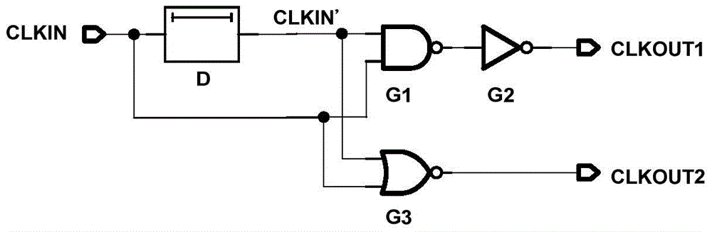
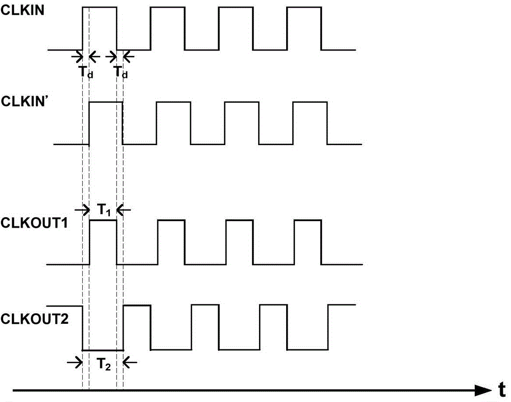
[0016] Such as figure 1 As shown, a two-phase non-overlapping clock signal generation circuit includes a delay unit D, a NAND gate G1, a NOR gate G2, and a NOR gate G3, wherein the master clock signal CLKIN generates a delayed clock signal through the delay unit D CLKIN', the delayed clock signal CLKIN' and the main clock signal CLKIN are input to the input terminal of the NAND gate G1, the output terminal of the NAND gate G1 is connected to the input terminal of the NOT gate G2, and the output signal of the NOT gate G2 is the first Clock signal CLKOUT1; delayed clock signal CLKIN' and the main clock signal are input to the input terminal of NOR gate ...
PUM
 Abstract
Description
Claims
Application Information
 - R&D
- Intellectual Property
- Life Sciences
- Materials
- Tech Scout
- Unparalleled Data Quality
- Higher Quality Content
- 60% Fewer Hallucinations
Browse by: Latest US Patents, China's latest patents, Technical Efficacy Thesaurus, Application Domain, Technology Topic, Popular Technical Reports.
© 2025 PatSnap. All rights reserved.Legal|Privacy policy|Modern Slavery Act Transparency Statement|Sitemap|About US| Contact US: help@patsnap.com