Semiconductor device and forming method thereof

A semiconductor and device technology, applied in the field of semiconductor devices and their formation, can solve the problems of easy leakage, poor ability of epitaxial filling, affecting device performance and reliability, etc., and achieve the requirements of ensuring high voltage performance and reliability and reducing requirements Effect

Active Publication Date: 2015-06-17
CHENGDU SILAN SEMICON MFG
View PDF5 Cites 3 Cited by
  • Summary
  • Abstract
  • Description
  • Claims
  • Application Information

AI Technical Summary

Problems solved by technology

Afterwards, the trench 12 is filled with an epitaxial layer using a conventional epitaxial filling process. Due to the deposition principle, during the epitaxial filling process, such as image 3 As shown, the atmosphere at the top of the trench is conducive to deposition so that the top of the trench is sealed first, so an epitaxial accumulation 13 is formed on the top of the trench 12, resulting in the internal space of the trench 12 not being filled and leaving a gap 13a. The closer the inclination θ1 is to 90 degrees, the worse the ability of epitaxial filling, the easier it is to form large gaps, and even large voids in severe cases
The existence of gaps and cavities makes the arrangement of silicon atoms and dopant atoms discontinuous to form defects, which leads to leakage easily during device operation, especially under high voltage conditions, and affects the performance and reliability of the device

Method used


Image

  • Semiconductor device and forming method thereof
  • Semiconductor device and forming method thereof
  • Semiconductor device and forming method thereof

Examples


Embodiment Construction

[0030] In order to make the above objects, features and advantages of the present invention more comprehensible, specific implementations of the present invention will be described in detail below in conjunction with the accompanying drawings.

[0031] In the following description, numerous specific details are set forth in order to provide a thorough understanding of the present invention. However, the present invention can be implemented in many other ways different from those described here, and those skilled in the art can make similar extensions without violating the connotation of the present invention, so the present invention is not limited by the specific implementations disclosed below.

[0032] see Figure 4 , the present invention provides a method for forming a semiconductor device, comprising the steps of:

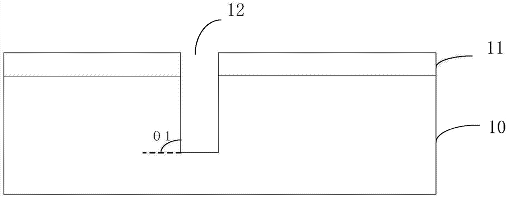
[0033] S11: providing a semiconductor substrate with a specific doping type;

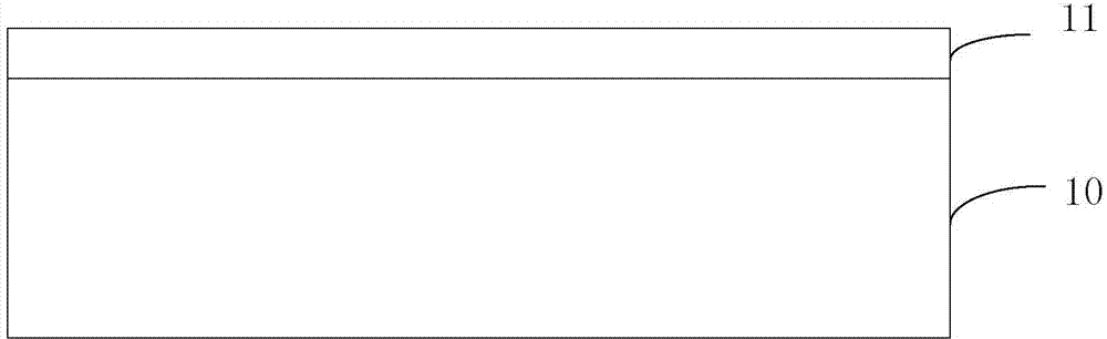
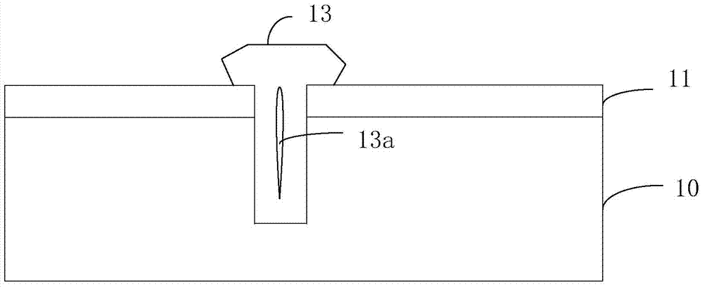
[0034] S12: forming a dielectric layer on the semiconductor substrate;

[0...


PUM


Abstract

The invention provides a semiconductor device and a forming method thereof. After a groove is formed in a semiconductor substrate of a specific doping type, the coating, baking and diffusing process is conducted through a latex doping source of the type opposite to the doping type of the semiconductor substrate, the groove is filled with the latex doping source which covers and repairs the surface of an oxidization layer, and meanwhile a doping area of the type opposite to the doping type of the semiconductor substrate is formed in the portion, around the groove, of the semiconductor substrate; a conventional extension doping process with complex processes and large technical difficulty is not needed, the groove is fully filled without defects, the requirement for the groove etching process is lowered, and the requirements for the high-voltage performance and reliability of the device are met.

Description

technical field [0001] The invention belongs to the technical field of semiconductor manufacturing technology, and relates to a semiconductor device and a forming method thereof. Background technique [0002] Super-junction MOSFET (Super-junction MOSFET) is a new type of power device. Due to its special vertical PN column alternating structure, the charges can compensate each other. When the device is in the off state, a lower voltage can be applied. The P-type region and the N-type region can achieve a higher breakdown voltage and lower on-resistance at the same time when a higher doping concentration is used. [0003] In the manufacturing process of superjunction devices, a semiconductor substrate of a specific doping type is usually formed first, and the opposite type of doping is performed on a specific region on the semiconductor substrate of the specific doping type, thereby forming a P-type region, an N-type intersecting superjunction structures. Taking the super-ju...

Claims


Application Information

Patent Timeline
Patent Type & Authority Applications(China)
IPC IPC(8): H01L21/336H01L29/06H01L29/78
Inventor 杨彦涛陈文伟李云飞陶玉美王伟
Owner CHENGDU SILAN SEMICON MFG
Why Eureka
Try Eureka