Developing apparatus and image forming apparatus
A developing device and developer technology, which are applied to the electric recording process using charge patterns, equipment and instruments of the electric recording process applying charge patterns, etc. The effect of preventing uneven concentration, preventing scattering, and providing sufficient sealing performance
- Summary
- Abstract
- Description
- Claims
- Application Information
AI Technical Summary
Problems solved by technology
Method used
Image
Examples
Embodiment
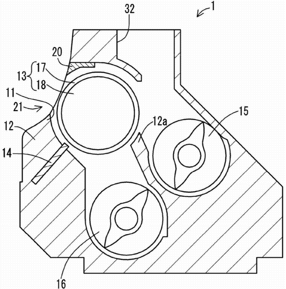
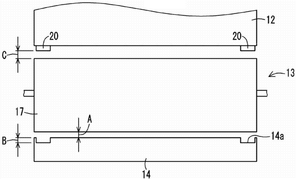
[0171] Use based on figure 1 For the developing device having the configuration shown in , the dimensions of the layer thickness regulating member 14 and the magnetic sealing member 20 were changed to evaluate toner scattering and the like.
[0172] A non-magnetic material made of SUS304 austenitic stainless steel was used as the material of the layer thickness regulating member 14 . The layer thickness regulating member 14 has a length of 330 mm and a width of 10 mm. The rectangular cutout 14 a is provided at a position facing the surface of the developing sleeve 17 corresponding to the non-image portion of the photoreceptor 3 so that the long side of the rectangle opens toward the developing sleeve 17 . The length of the long side of the cutout 14a is 5 mm.
[0173] As the material of the magnetic sealing member 20, SUS430 was used. The magnetic seal member 20 is provided at a position facing the surface of the developing sleeve 17 corresponding to the photoreceptor 3 on ...
PUM
 Abstract
Description
Claims
Application Information


