A full reinforcement method and system for anti-single event flipping of semiconductor circuits

An anti-single particle and semiconductor technology, applied in logic circuits, electrical components, electrical digital data processing, etc., can solve the problems of poor reinforcement effect and low efficiency of design methods, and achieve guaranteed reinforcement effect, fast simulation speed, and simple operation. Effect

Active Publication Date: 2018-01-26
SHENZHEN STATE MICROELECTRONICS CO LTD
View PDF3 Cites 0 Cited by
  • Summary
  • Abstract
  • Description
  • Claims
  • Application Information

AI Technical Summary

Problems solved by technology

[0007] The purpose of the embodiments of the present invention is to provide a full reinforcement method for anti-single event flipping of semiconductor circuits, aiming to solve the problems of low efficiency and poor reinforcement effect of the current simulation and design methods for full reinforcement anti-single event flipping in semiconductor circuits

Method used


Image

  • A full reinforcement method and system for anti-single event flipping of semiconductor circuits
  • A full reinforcement method and system for anti-single event flipping of semiconductor circuits
  • A full reinforcement method and system for anti-single event flipping of semiconductor circuits

Examples


Embodiment Construction

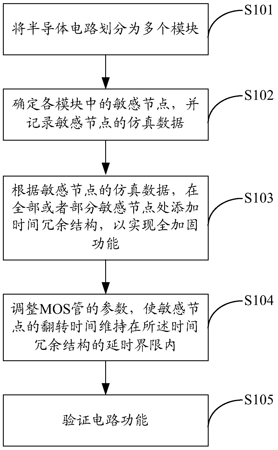
[0037] In order to make the object, technical solution and advantages of the present invention clearer, the present invention will be further described in detail below in conjunction with the accompanying drawings and embodiments. It should be understood that the specific embodiments described here are only used to explain the present invention, not to limit the present invention.

[0038] In the embodiment of the present invention, the circuit is divided into blocks before the simulation, and the sensitive nodes in each module are respectively determined, so as to add a time redundant structure to the sensitive nodes, realize the full reinforcement function, and further enhance by adjusting the parameters of the MOS tube The reinforcement effect reaches the design standard of full reinforcement, the operation is simple, the increased circuit area is small, and the increased power consumption is low.

[0039] The realization of the present invention is described in detail belo...


PUM


Abstract

The present invention is applicable to the field of semiconductors, and provides a method and system for fully strengthening semiconductor circuits against single event flipping. The method includes: dividing the semiconductor circuit into multiple modules; determining sensitive nodes in each module, and recording the sensitive The simulation data of the node; according to the simulation data of the sensitive node, add a time redundancy structure at all or part of the sensitive node to realize the full reinforcement function; adjust the parameters of the MOS tube to maintain the flipping time of the sensitive node Within the delay bounds of the time redundancy structure; verifying circuit functionality. In the present invention, the circuit is divided into blocks before simulation, and the sensitive nodes in each module are respectively determined, so as to add a time redundant structure to the sensitive nodes, realize the full reinforcement function, and further enhance the reinforcement effect by adjusting the parameters of the MOS tube , to achieve the design standard of full reinforcement, simple operation, small increase in circuit area, and low increase in power consumption.

Description

technical field [0001] The invention belongs to the field of semiconductors, and in particular relates to a full reinforcement method and system for semiconductor circuits against single event flipping. Background technique [0002] A large number of semiconductor chips are integrated in modern aerospace systems. Because the earth and the universe are full of various energetic particles, these high-energy particles penetrate the chip shell and transmit to the sensitive area of ​​the semiconductor circuit. Due to the instantaneous energy transmission of a single particle, the chip The voltage of a certain area or node jumps instantaneously, causing the logic state of the digital circuit to change instantaneously, that is, a single event flip occurs. [0003] With the continuous advancement of semiconductor technology, single event upset has become the main cause of chip failure and errors in aerospace systems. Submicron semiconductor chips below 0.13um process are especially ...

Claims


Application Information

Patent Timeline
Patent Type & Authority Patents(China)
IPC IPC(8): G06F17/50H03K19/094
Inventor 黎陈波邱嘉敏罗春华李孝远
Owner SHENZHEN STATE MICROELECTRONICS CO LTD
Why Eureka
Try Eureka