Supercharge Your Innovation With Domain-Expert AI Agents!

Chip electronic component and manufacturing method thereof

A technology of electronic components and manufacturing methods, applied in the direction of inductance/transformer/magnet manufacturing, coil manufacturing, electrical components, etc., capable of solving problems such as high aspect ratio limitations, increased coil pattern spacing, and coil pattern short circuits

Active Publication Date: 2015-06-24
SAMSUNG ELECTRO MECHANICS CO LTD
View PDF12 Cites 19 Cited by
  • Summary
  • Abstract
  • Description
  • Claims
  • Application Information

AI Technical Summary

Problems solved by technology

[0009] However, in the case of forming the inner coil by the existing pattern plating method using a plating resist, in order to increase the thickness of the coil pattern, the thickness of the plating resist should be increased, and the plating resist having the increased thickness should Having a predetermined width or more to maintain its shape, causing problems such as increased spacing between coil patterns
[0010] In addition, when the inner coil is formed using the electroplating process according to the related art, since the coil pattern grows isotropically in the width and thickness directions of the coil pattern, a short circuit may occur between the coil patterns, and the relatively high height of the coil may be achieved. There will be limitations in terms of aspect ratio (AR)

Method used


Image

  • Chip electronic component and manufacturing method thereof
  • Chip electronic component and manufacturing method thereof
  • Chip electronic component and manufacturing method thereof

Examples


Embodiment Construction

[0036] Exemplary embodiments of the present disclosure will now be described in detail with reference to the accompanying drawings.

[0037] This disclosure, however, may be embodied in many different forms and should not be construed as limited to the specific embodiments set forth herein. Rather, these embodiments are provided so that this disclosure will be thorough and complete, and will fully convey the scope of the disclosure to those skilled in the art.

[0038] In the drawings, the shapes and dimensions of elements may be exaggerated for clarity, and the same reference numerals will be used throughout to designate the same or like elements.

[0039] chip electronic components

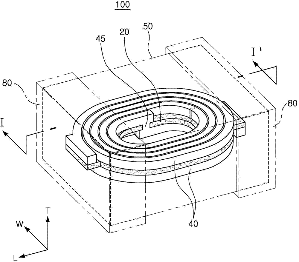
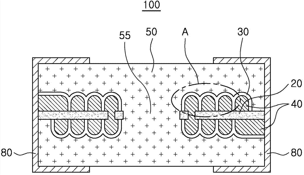
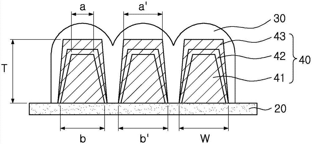
[0040] Hereinafter, a chip type electronic component according to an exemplary embodiment of the present disclosure will be described. For example, a thin film type inductor will be described, but the present disclosure is not limited thereto.

[0041] figure 1 is a schematic perspective v...


PUM

PropertyMeasurementUnit
widthaaaaaaaaaa
widthaaaaaaaaaa
thicknessaaaaaaaaaa

Abstract

There are provided a chip electronic component comprising: a magnetic body including an insulation substrate; an internal coil part formed on at least one surface of the insulation substrate; and an external electrode formed on an end surface of the magnetic body and connected to the internal coil part, wherein the internal coil part includes a first coil pattern formed on the insulation substrate and a second coil pattern formed to coat the first coil pattern, and a ratio a / b of a width a of an upper surface of the first coil pattern with respect to a width b of a lower surface of the first coil pattern is less than 1.

Description

[0001] This application claims the benefit of Korean Patent Application No. 10-2013-0158078 filed in the Korean Intellectual Property Office on December 18, 2013, the disclosure of which is hereby incorporated by reference. technical field [0002] The present disclosure relates to a chip electronic component and a manufacturing method thereof. Background technique [0003] Inductors, which are chip electronic components, are representative passive components that constitute electronic circuits together with resistors and capacitors to remove noise. The inductor is combined with a capacitor using electromagnetic properties to constitute a resonance circuit, a filter circuit, etc. that amplify a signal of a specific frequency band. [0004] Recently, since miniaturization and slimming of information technology (IT) devices such as various communication devices, display devices, etc. Research on technologies for thinning and thinning has been continuously carried out. Induct...

Claims


Application Information

Patent Timeline
Patent Type & Authority Applications(China)
IPC IPC(8): H01F17/04H01F27/28H01F41/00H01F41/04
CPCC25D5/022C25D5/10H01F17/0013H01F27/292H01F41/046H01F2017/048C25D7/001
Inventor 郑东晋金省勋闵炳承
Owner SAMSUNG ELECTRO MECHANICS CO LTD
Features
  • R&D
  • Intellectual Property
  • Life Sciences
  • Materials
  • Tech Scout
  • Unparalleled Data Quality
  • Higher Quality Content
  • 60% Fewer Hallucinations
Learn More