Fin-type field effect transistor forming method
A fin-type field effect and transistor technology, which is applied in semiconductor devices, semiconductor/solid-state device manufacturing, electrical components, etc., can solve problems affecting FinFET performance and achieve the effect of avoiding adverse effects
- Summary
- Abstract
- Description
- Claims
- Application Information
AI Technical Summary
Problems solved by technology
Method used
Image

Examples
Embodiment Construction
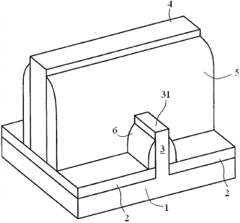
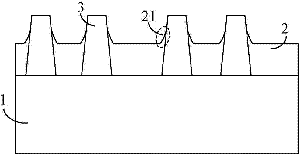
[0033] As mentioned in the background technology, during the fabrication of FinFETs, during the process of etching the oxide layer covering the top of the fins to expose part of the height of the fins, there will be some residual oxidation on the sidewalls of the fins. object layer. This part of the oxide layer will directly affect the performance of the subsequently formed FinFET. Analyzing the reason, it may be that, in the fabrication process of the fin field effect transistor, based on the structural requirements of the fin field effect transistor to be formed and the influence of process conditions, the density of the oxide formed on the fin is different, based on The difference in the density of the oxide layer in different parts causes the difference in the etching rate of the oxide layer in different parts of subsequent etching. Typical examples such as:
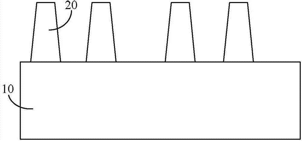
[0034] In the manufacturing process of the fin field effect transistor, the formation process of the oxide layer...
PUM
 Abstract
Description
Claims
Application Information
 - R&D
- Intellectual Property
- Life Sciences
- Materials
- Tech Scout
- Unparalleled Data Quality
- Higher Quality Content
- 60% Fewer Hallucinations
Browse by: Latest US Patents, China's latest patents, Technical Efficacy Thesaurus, Application Domain, Technology Topic, Popular Technical Reports.
© 2025 PatSnap. All rights reserved.Legal|Privacy policy|Modern Slavery Act Transparency Statement|Sitemap|About US| Contact US: help@patsnap.com