Method for locating double-bit line bridge connection

A bit line and bridging technology, which is applied in the direction of electrical components, circuits, semiconductor/solid-state device testing/measurement, etc., can solve problems such as damage, miss, and inability to apply double bit line bridging, etc., to overcome time-consuming problems and overcome easy damage faint bridge effect

Active Publication Date: 2015-06-24
WUHAN XINXIN SEMICON MFG CO LTD
View PDF3 Cites 0 Cited by
  • Summary
  • Abstract
  • Description
  • Claims
  • Application Information

AI Technical Summary

Problems solved by technology

[0002] At present, the VC (voltage contrast, VC for short) method is used to locate the failure location of storage products containing buried bit lines, but this method cannot be applied to the failure analysis of double bit line bridges. In order to effectively locate the double bit line bridges For the failure position, we use the method of SEM (Scanning Electron Microsoft, scanning electron microscope, referred to as SEM) to scan the entire bit line in a carpet manner. This method meets the needs of users to a certain extent, and has substantial advantages compared with the previous technology improvement
[0003] But this method is very time-consuming, and weak bridges (can be but not limited to bonded wire bridges), easily missed in SEM scans or destroyed by RIE (Reactive Ion Etching, reactive ion etching, referred to as RIE)

Method used


Image

  • Method for locating double-bit line bridge connection
  • Method for locating double-bit line bridge connection
  • Method for locating double-bit line bridge connection

Examples


Embodiment Construction

[0034] The present invention will be further described below in conjunction with the accompanying drawings and specific embodiments, but not as a limitation of the present invention.

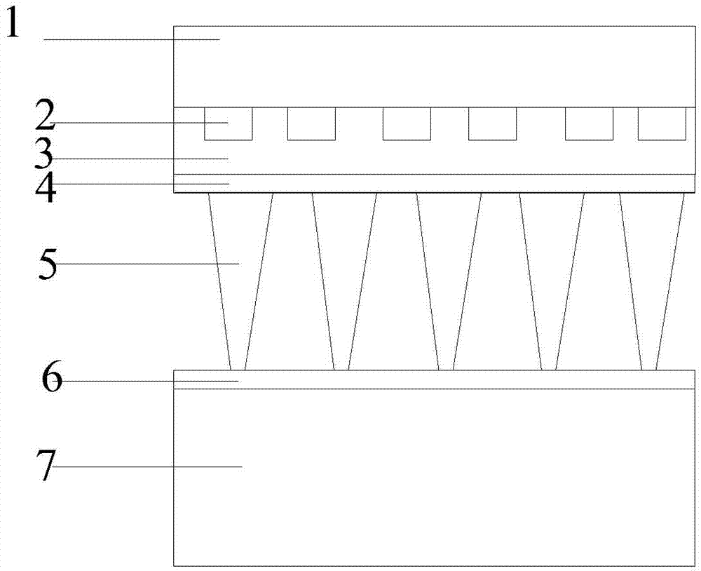
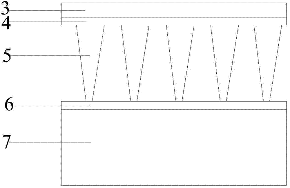
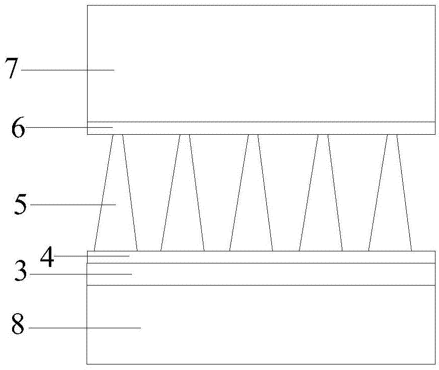
[0035] see figure 1 As shown in the structure, a failure sample is provided, and the failure sample includes a substrate 7 having a front surface and a back surface opposite to the front surface, and buried bit lines are sequentially stacked on the front surface of the substrate from bottom to top Layer 6, dielectric layer 5, first metal layer 4, first interlayer dielectric layer 3 and second interlayer dielectric layer 1, bit lines are arranged in the first metal layer 4, and bit lines in the first metal layer 4 are connected to The bit lines in the buried bit line layer 6 are connected by connection lines, and the buried bit line layer is connected to the first metal layer by several connection lines penetrating through the dielectric layer, and is adjacent to the first interlayer dielectric l...


PUM


Abstract

The invention relates to the technical field of semiconductor manufacturing, in particular to a method for locating double-bit line bridge connection. A carrier silicon wafer is added, one of the double-bit lines is connected with the carrier silicon wafer, then the double-bit lines are cut piecewise, and the double-bit line bridge connection position is judged according to the bright and dim degree of an image of the bit lines. By means of the technical scheme of the method for locating the double-bit line bridge connection, locating of the double-bit line bridge connection is achieved rapidly and efficiently, and the problems of time consumption in traditional locating of the double-bit line bridge failure position and easily caused damage to a weak bridge are solved.

Description

technical field [0001] The invention relates to the technical field of semiconductor manufacturing, in particular to a method for positioning double bit line bridges. Background technique [0002] At present, the VC (voltage contrast, VC for short) method is used to locate the failure location of storage products containing buried bit lines, but this method cannot be applied to the failure analysis of double bit line bridges. In order to effectively locate the double bit line bridges For the failure position, we use the method of SEM (Scanning Electron Microsoft, scanning electron microscope, referred to as SEM) to scan the entire bit line in a carpet manner. This method meets the needs of users to a certain extent, and has substantial advantages compared with the previous technology improvement. [0003] But this method is very time-consuming, and weak bridges (which can be but not limited to bonded wire bridges) are easily missed in SEM scans or destroyed by RIE (Reactive...

Claims


Application Information

Patent Timeline
Patent Type & Authority Applications(China)
IPC IPC(8): H01L21/66
CPCH01L22/22
Inventor 李桂花仝金雨刘君芳郭伟李品欢
Owner WUHAN XINXIN SEMICON MFG CO LTD
Why Eureka
Try Eureka