
High-voltage light-emitting diode and manufacturing method thereof

A technology of high-voltage lighting and manufacturing methods, which is applied in the direction of electrical components, circuits, semiconductor devices, etc., can solve the problems of poor stability, poor consistency, and low yield of high-voltage LEDs, so as to increase reliability and life, improve light efficiency, and improve The effect of yield rate and production line pass rate

Active Publication Date: 2015-06-24
XIANGNENG HUALEI OPTOELECTRONICS
View PDF3 Cites 11 Cited by
  • Summary
  • Abstract
  • Description
  • Claims
  • Application Information

AI Technical Summary

Benefits of technology

This new technology improves the performance of high voltage light emitter devices while reducing their cost compared to current methods. It also increases productivity without sacrificing quality or durability over time.

Problems solved by technology

This patented describes a way to improve the performance and efficiency of Light Emitted Devices (LED). Highly efficient devices use less expensive materials while maintain their brightness over time due to improved electronics made possible at very large scales. By breaking down traditional methods for creation of packages containing multiple components together, the resulting package can achieve higher levels of durableity without compromising on overall functionality or usages compared to previous designs.

Method used


Image

  • High-voltage light-emitting diode and manufacturing method thereof
  • High-voltage light-emitting diode and manufacturing method thereof
  • High-voltage light-emitting diode and manufacturing method thereof

Examples


Embodiment Construction

[0036] Certain terms are used, for example, in the description and claims to refer to particular components. Those skilled in the art should understand that hardware manufacturers may use different terms to refer to the same component. The specification and claims do not use the difference in name as a way to distinguish components, but use the difference in function of components as a criterion for distinguishing. As mentioned throughout the specification and claims, "comprising" is an open term, so it should be interpreted as "including but not limited to". "Approximately" means that within an acceptable error range, those skilled in the art can solve the technical problem within a certain error range and basically achieve the technical effect. The subsequent description of the specification is a preferred implementation mode for implementing the application, but the description is for the purpose of illustrating the general principle of the application, and is not intended...


PUM


Abstract

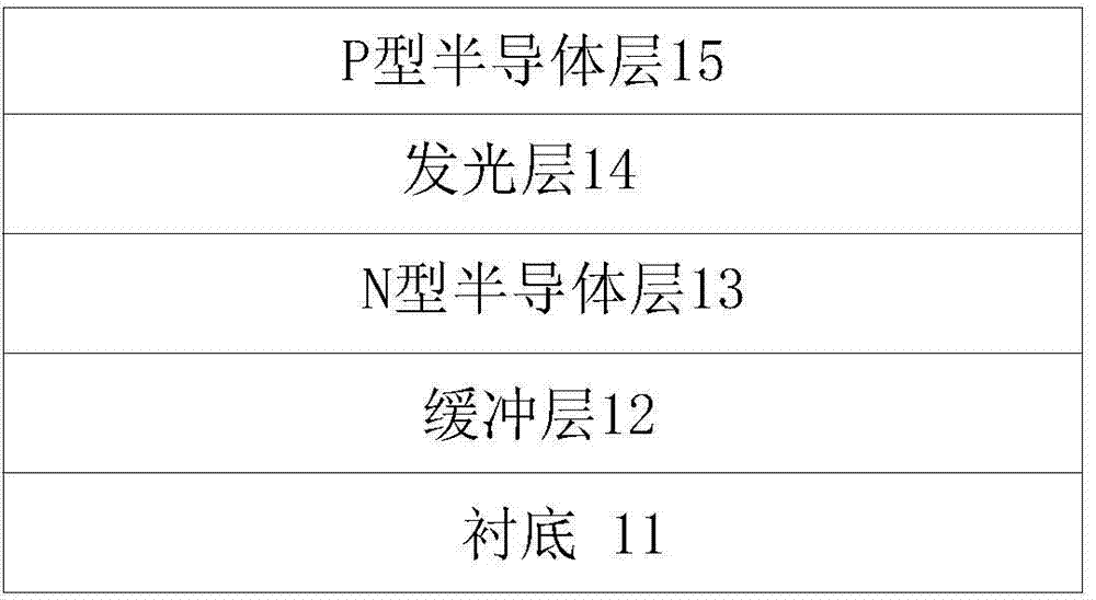
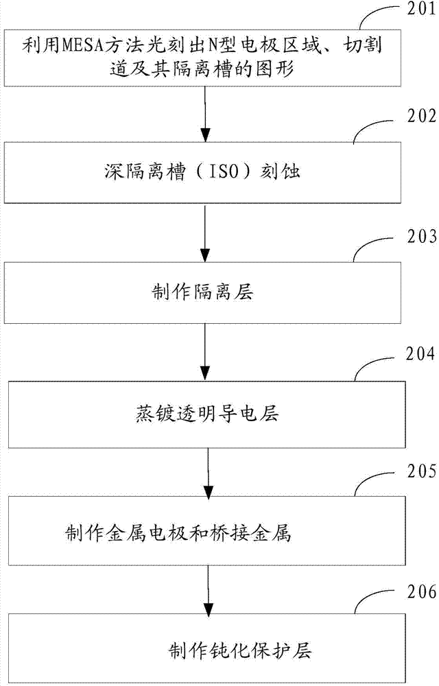
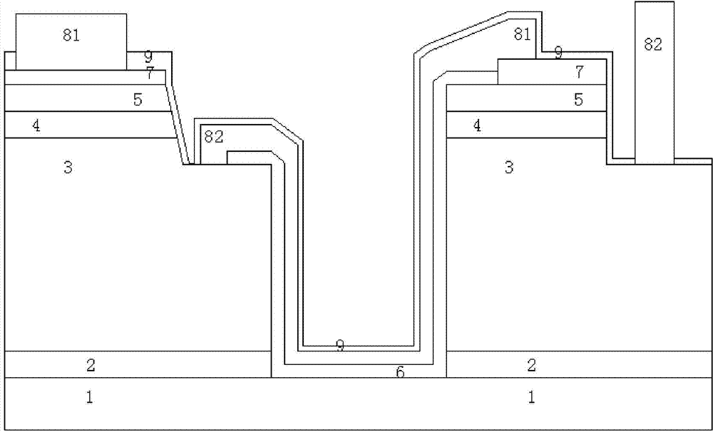
The invention discloses a high-voltage light-emitting diode and a manufacturing method thereof. The high-voltage light-emitting diode is obtained by processing a substrate. The substrate comprises a liner, a buffer layer located on the liner, an N type GaN layer located on the buffer layer, a light-emitting layer located on the N type GaN layer, and a P type GaN layer located on the light-emitting layer. The method includes the steps of plating the substrate with a transparent conductive layer in an evaporation mode, photo-etching patterns of an N type electrode area, a cutting channel and an isolation groove through an MESA method, etching the isolation groove to form an isolation layer, manufacturing a metal electrode and bridging metal, and manufacturing a passivated protecting layer. By means of the high-voltage light-emitting diode and the manufacturing method thereof, the high-voltage light-emitting diode manufacturing process is simplified; the high-voltage light-emitting diode yield and production line first pass yield are increased; the reliability of the high-voltage light-emitting diode is improved, and the service life of the high-voltage light-emitting diode is prolonged; the luminous efficacy of the high-voltage light-emitting diode is improved.

Description


Claims


Application Information

Patent Timeline
Owner XIANGNENG HUALEI OPTOELECTRONICS
Learn More