Wafer processing system and wafer processing method
A technology of silicon wafer and control system
- Summary
- Abstract
- Description
- Claims
- Application Information
AI Technical Summary
Problems solved by technology
Method used
Image


Examples
Embodiment Construction
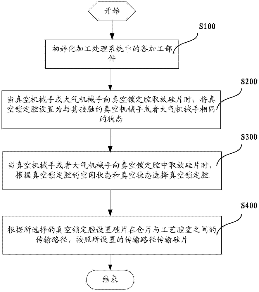
[0051]In order to make the object, technical solution and advantages of the present invention more clear, the specific implementation of the silicon wafer processing system and method according to the embodiment of the present invention will be described below with reference to the accompanying drawings. It should be understood that the specific embodiments described here are only used to explain the present invention, not to limit the present invention.
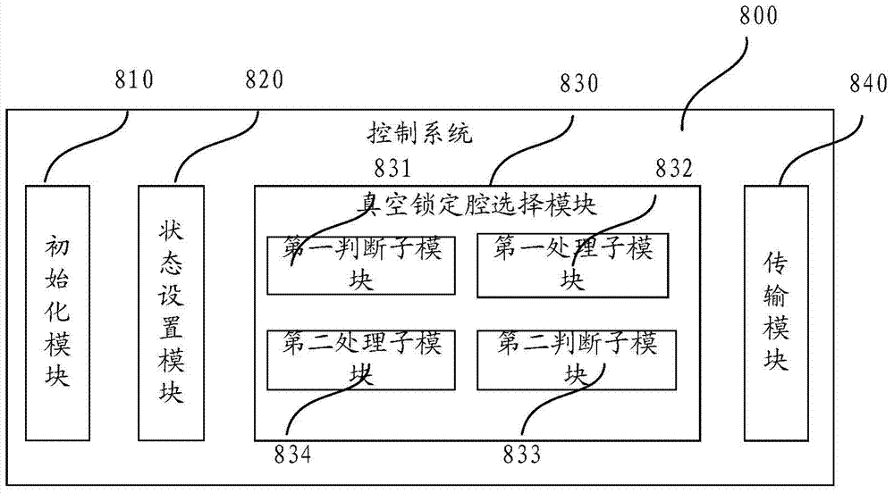
[0052] A system for processing silicon wafers according to an embodiment of the present invention, such as figure 1 , figure 2 As shown, it includes: a process chamber 700, a transfer device and a control system 800;
[0053] The silicon wafer processing system transports silicon wafers to the process chamber 700 in the silicon wafer processing engineering.
[0054] The transfer device performs specific silicon wafer transfer tasks, including a wafer bin 100, an atmospheric manipulator 300, a vacuum manipulator 600 and a ...
PUM
 Abstract
Description
Claims
Application Information
 - R&D
- Intellectual Property
- Life Sciences
- Materials
- Tech Scout
- Unparalleled Data Quality
- Higher Quality Content
- 60% Fewer Hallucinations
Browse by: Latest US Patents, China's latest patents, Technical Efficacy Thesaurus, Application Domain, Technology Topic, Popular Technical Reports.
© 2025 PatSnap. All rights reserved.Legal|Privacy policy|Modern Slavery Act Transparency Statement|Sitemap|About US| Contact US: help@patsnap.com