Reaction chamber and plasma processing device

A reaction chamber and plasma technology, which is applied in semiconductor/solid-state device manufacturing, conveyor objects, discharge tubes, etc., can solve problems such as difficulty in guaranteeing verticality of thimble 42, cumbersome debugging process, and influence on levelness, etc., to achieve simple structure , Reduced drive unit, easy to control the effect

Active Publication Date: 2015-07-01
BEIJING NAURA MICROELECTRONICS EQUIP CO LTD
View PDF4 Cites 3 Cited by
  • Summary
  • Abstract
  • Description
  • Claims
  • Application Information

AI Technical Summary

Problems solved by technology

[0005] The above-mentioned reaction chamber 1 drives the base 3 through the first driving device 6, and the thimble mechanism 4 is driven by the second driving device 7. Cooperating with the manipulator / third driving device 8, the transmission of the processed workpiece / shielding disk 5 is realized, but the process is very complicated. ; Moreover, there are many controls involving the first drive device 6, the second drive device 7 and the manipulator, resulting in a cumbersome debugging process
[0006] In addition, in the above-mentioned reaction chamber 1, the second driving device 7 is connected to the edge position of the thimble base 41 with the thimble mechanism 4, so that the thimble base 41 forms a cantilever structure. In this case, the verticality of the plurality of thimbles 42 is difficult. Guaranteed, which will affect the levelness of the processed workpiece when it is placed on the thimble mechanism 4

Method used


Image

  • Reaction chamber and plasma processing device
  • Reaction chamber and plasma processing device
  • Reaction chamber and plasma processing device

Examples


Embodiment Construction

[0035] In order for those skilled in the art to better understand the technical solution of the present invention, the reaction chamber and plasma processing equipment provided by the present invention will be described in detail below with reference to the accompanying drawings.

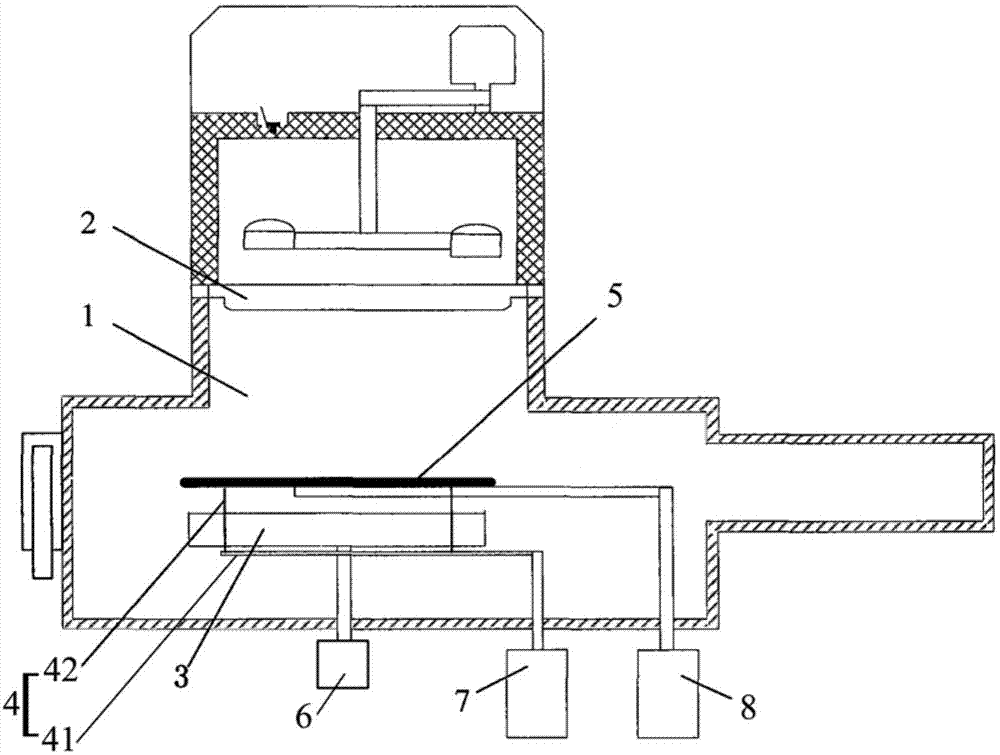
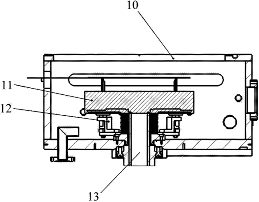
[0036] figure 2Schematic diagram of the structure of the reaction chamber provided by the embodiment of the present invention. image 3 for figure 2 The perspective schematic diagram of the carrying device and the thimble mechanism in the shown reaction chamber. Figure 4 for figure 2 Schematic cross-sectional view of the carrying device and the thimble mechanism in the shown reaction chamber. Please also see figure 2 , image 3 and Figure 4 , the reaction chamber 10 is used to process the workpiece to be processed, and a carrying device 11 and a thimble mechanism 12 are arranged in it. Wherein, the carrying device 11 is provided with a plurality of vertical passages 110, in the present ...


PUM


Abstract

The invention relates to a reaction chamber and a plasma processing device. The reaction chamber is internally provided with a loading device and an ejector pin mechanism, wherein the ejector pin mechanism comprises a supporting part and a plurality of ejector pin assemblies; each ejector pin assembly comprises an ejector pin, a compressing spring, a baffle and a limiting block; each ejector pin is arranged on the supporting part and corresponding to one vertical channel in the vertical direction; a vertical first concave hole is formed below each ejector pin; each compressing spring is arranged in each concave hole, and the top end of each compressing spring is in contact with the top wall of an annular concave part in order to provide a vertical elasticity to drive each ejector pin to raise; a first step and a second step are arranged on the peripheral wall of each ejector pin, wherein the first step is positioned above the second step; the baffles are arranged on the first steps; the limiting blocks are fixed on the supporting part, comprising coiling parts which coil the ejector pins and are positioned between the first steps and the second steps. According to the reaction chamber, a processed workpiece can be simply transmitted, the structure is simple, and therefore, the transmission process is easily controlled, and the manufacturing cost is reduced.

Description

technical field [0001] The invention relates to the field of semiconductor equipment manufacturing, in particular to a reaction chamber and plasma processing equipment. Background technique [0002] figure 1 It is a structural schematic diagram of a reaction chamber of an existing Physical Vapor Deposition (Physical Vapor Deposition, hereinafter referred to as PVD) equipment. Such as figure 1 As shown, the reaction chamber 1 of the PVD equipment is provided with a target 2 , a base 3 , a thimble mechanism 4 , a shielding plate 5 , a first driving device 6 , a second driving device 7 and a third driving device 8 . Wherein, the base 3 is used to carry the workpiece to be processed. The first driving device 6 is arranged under the base 3 and is used to drive the base 3 to move up and down in the vertical direction. The thimble mechanism 4 is arranged below the base 3, and it includes a thimble base 41 and a plurality of thimbles 42; the second driving device 7 is connected ...

Claims


Application Information

Patent Timeline
IPC IPC(8): H01L21/687H01L21/677H01J37/34
CPCH01J37/34H01L21/67703H01L21/67739H01L21/67766H01L21/68785
Inventor 王涛
Owner BEIJING NAURA MICROELECTRONICS EQUIP CO LTD
Why Eureka
Try Eureka