Automatic wafer conveying device

A wafer transfer device and wafer wafer technology, which is applied in the manufacture of semiconductor/solid-state devices, electrical components, circuits, etc., can solve the problems of manual transmission force cannot be mastered, labor-intensive, fragmentation, etc., to achieve easy operation, avoid wafer The effect of dislocation of wafers and avoiding damage to transfer wafers

Pending Publication Date: 2022-04-05
博福特(厦门)新材料有限公司
View PDF0 Cites 0 Cited by
  • Summary
  • Abstract
  • Description
  • Claims
  • Application Information

AI Technical Summary

Problems solved by technology

[0003] In the existing wafer production process, it needs to be transferred from one production process to the next production process. In the existing technology, manual transmission is relied on. The transmission process consumes a lot of manpower, and the manual transmission force cannot be mastered, which is easy to cause fragments

Method used


Image

  • Automatic wafer conveying device
  • Automatic wafer conveying device
  • Automatic wafer conveying device

Examples


Embodiment 1

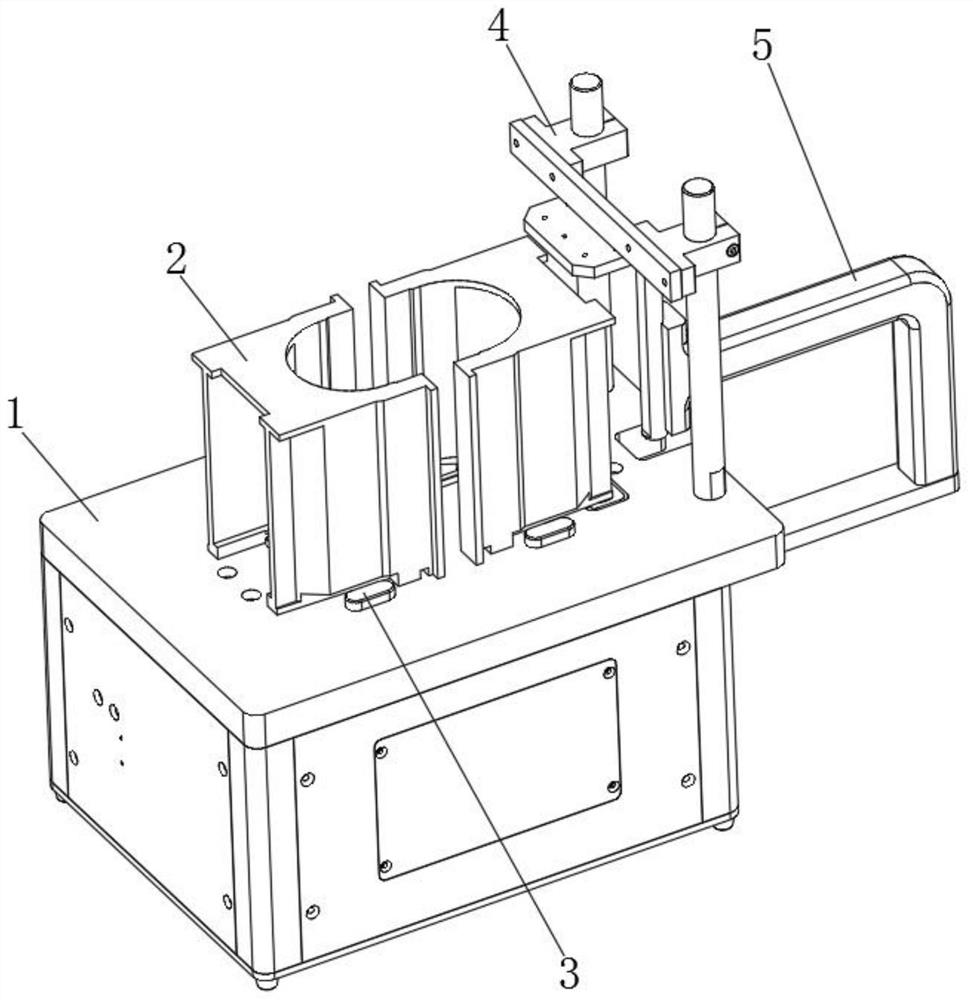
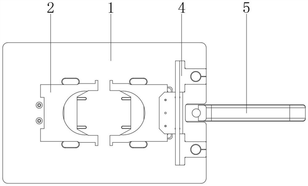
[0038] When the wafer is transferred, the cassette 2 with the wafer and the empty cassette 2 are respectively loaded on the top of the equipment box 1. When installing, the two flat sides 22 at the bottom of the cassette 2 are snapped into the limit position In the gap between the block 32 and the positioning protrusion 31, and make the cassette 2 with the wafer close to the pushing mechanism 5, and make the rib 21 of the cassette 2 snap into the limit groove 33, thereby realizing The horizontal and vertical positioning of the cassette 2, and after the installation of the cassette 2 is completed, the cassette 2 squeezes the positioning cylinder 34, so that the positioning cylinder 34 squeezes the pressure sensor, so that the film transfer device can work normally;

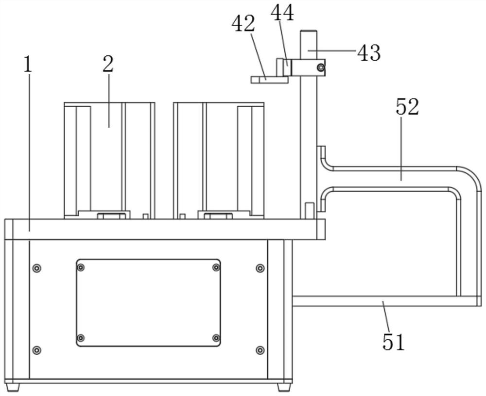
[0039] After the cassette 2 is installed, the infrared transmitter 41 sends an infrared signal. When the infrared receiver 42 receives the signal, the device works normally. When the infrared receiver 42 does not re...


PUM


Abstract

The invention relates to the technical field of wafer production, in particular to an automatic wafer transfer device, which comprises an equipment box body and two groups of clamping boxes, wafers are arranged in one group of clamping boxes, the other group of clamping boxes are empty clamping boxes, and two groups of clamping box positioning structures are arranged at the top of the equipment box body; a detection mechanism is arranged at the top of the equipment box body, and the detection mechanism is used for detecting the orientation of the wafer in the cartridge filled with the wafer; the top of the equipment box body is provided with a material pushing mechanism, the material pushing mechanism is used for conveying the wafer in the cartridge containing the wafer into another group of empty cartridges, the cartridge can be accurately positioned through the cartridge positioning structure when the wafer is conveyed, then the position of the wafer in the cartridge is detected through the detection mechanism, dislocation of the wafer is avoided, and the wafer conveying efficiency is improved. The whole conveying process is simple and easy to operate, automatic wafer conveying is achieved, the wafers can be detected, and wafer conveying damage caused by dislocation of the wafers is avoided.

Description

technical field [0001] The invention relates to the technical field of wafer production, in particular to an automatic wafer transfer device. Background technique [0002] Elemental silicon is a gray, brittle, tetravalent, non-metallic chemical element. 27.8% of the earth's crust is composed of silicon, second only to oxygen, and silicon is a relatively abundant element in nature. Silicon is found in quartz, agate, flint and common beach rocks. Silicon wafers, also known as wafers, are processed from silicon ingots. Millions of transistors can be etched on silicon wafers through special processes, and are widely used in the manufacture of integrated circuits. [0003] In the existing wafer production process, it is necessary to transfer from one production process to the next production process. In the existing technology, manual transmission is relied on. The transmission process consumes a lot of manpower, and the manual transmission force cannot be mastered, which is ea...

Claims


Application Information

Patent Timeline
IPC IPC(8): H01L21/677H01L21/68
Inventor 段克波
Owner 博福特(厦门)新材料有限公司
Why Eureka
Try Eureka