NAND FLASH bad block management system and method
A management method and management system technology, applied in the field of integrated circuit storage, to achieve the effect of improving effectiveness, improving accuracy and improving efficiency
- Summary
- Abstract
- Description
- Claims
- Application Information
AI Technical Summary
Problems solved by technology
Method used
Image


Examples
Embodiment Construction
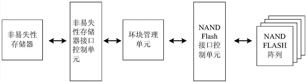
[0032] Such as figure 1 As shown, the present invention includes an interface control unit of NAND FLASH, an interface control unit of nonvolatile memory and a bad block management unit. Non-volatile memory can bring higher data validity to EEPROM than conventional writing in the OOB area of NAND FLASH.
[0033] Such as figure 2 As shown, traverse each block (Block) unit of the NAND FLASH array in the order of increasing block address (Block Address), check the first OOB area of the current block (Block), if the first byte (Byte) of the area It is 8'h00, indicating that the Block unit is a bad block. If it is not 8'h00, then perform an erase operation on the block. If the status register shows that the erase is successful, then perform bit error detection, otherwise program the first byte (Byte) data of the first OOB area to 8' h00 is used to mark the bad block, and the block (Block) represented by the address is marked as a bad block in the bad block table of the embe...
PUM
 Abstract
Description
Claims
Application Information