
Overlay alignment mark and overlay measurement method
A technology for aligning marks and markings, applied in the field of semiconductors, can solve problems such as poor measurement accuracy, and achieve the effect of improving measurement accuracy
Patent Information
- Authority / Receiving Office
- CN · China
- Patent Type
- Patents(China)
- Current Assignee / Owner
- Publication Date
- 2018-06-01
Smart Images
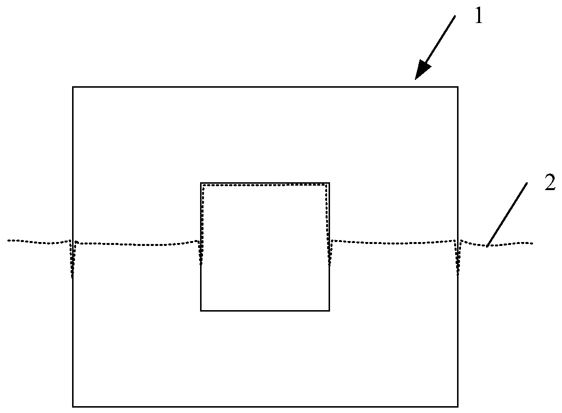
Figure 1 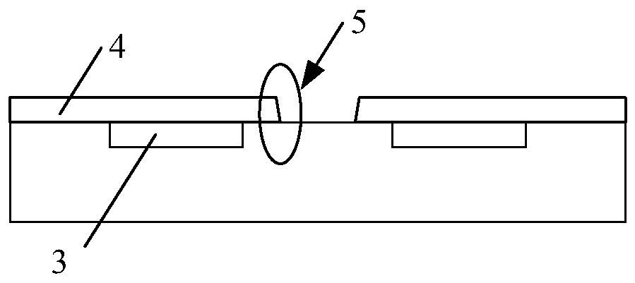
Figure 2 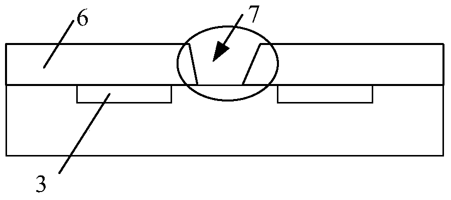
Figure 3
Abstract
Description
technical field
[0001] The invention relates to the technical field of semiconductors, in particular to an overlay alignment mark and an overlay measurement method. Background technique
[0002] In the semiconductor manufacturing process, the photolithography process has been developed as the core technology of each technology generation. In the standard CMOS process, dozens of photolithography steps are required, and the factors affecting the error of the photolithography process are not only the resolution of the photolithography machine, but also the accuracy of alignment. That is to say, each layer must be aligned with the previous layer within a certain range, that is, the overlay (OVL) accuracy must meet the design requirements.
[0003] Such as figure 1 As shown, in the prior art, the overlay measurement is to use the measuring equipment to capture the boundary signal 2 of the overlay mark 1, so as to know whether the alignment is accurate.
[0004] In the photolit...
Examples
Embodiment Construction
[0027] The overlay alignment mark and overlay measurement method of the present invention will be described in more detail below in conjunction with schematic diagrams, wherein a preferred embodiment of the present invention is shown, and it should be understood that those skilled in the art can modify the present invention described herein while still The advantageous effects of the present invention are realized. Therefore, the following description should be understood as the broad knowledge of those skilled in the art, but not as a limitation of the present invention.
[0028] In the interest of clarity, not all features of an actual implementation are described. In the following description, well-known functions and constructions are not described in detail since they would obscure the invention with unnecessary detail. It should be appreciated that in the development of any actual embodiment, numerous implementation details must be worked out to achieve the developer's ...