Wafer processing method

A processing method and chip technology, applied in stone processing equipment, fine working devices, manufacturing tools, etc., can solve problems such as deterioration of bending strength, difficulty in forming chips, chip damage, etc., and achieve the effect of deterioration of bending strength

Active Publication Date: 2019-07-02
DISCO CORP
View PDF5 Cites 0 Cited by
  • Summary
  • Abstract
  • Description
  • Claims
  • Application Information

AI Technical Summary

Problems solved by technology

[0009] However, in the scribing first thinning method of cited document 1, there is a problem that if a half-cut groove having a depth of half or more of the wafer thickness is formed, a protective tape needs to be pasted on the front surface of the wafer after the groove is formed. The protective tape is used to protect the device formed on the front side during the subsequent backside grinding, but the wafer will be damaged during the operation when attaching the protective tape
[0010] In addition, in the SDBG method of Cited Document 2, there is also the following problem: since the crack layer that can extend from one altered layer is about 150 μm, if the altered layer is not left on the side surface of the chip after grinding in order to avoid deterioration of the bending strength , it is difficult to form a chip with a thickness of 150 μm or more

Method used


Image

  • Wafer processing method
  • Wafer processing method
  • Wafer processing method

Examples


Embodiment Construction

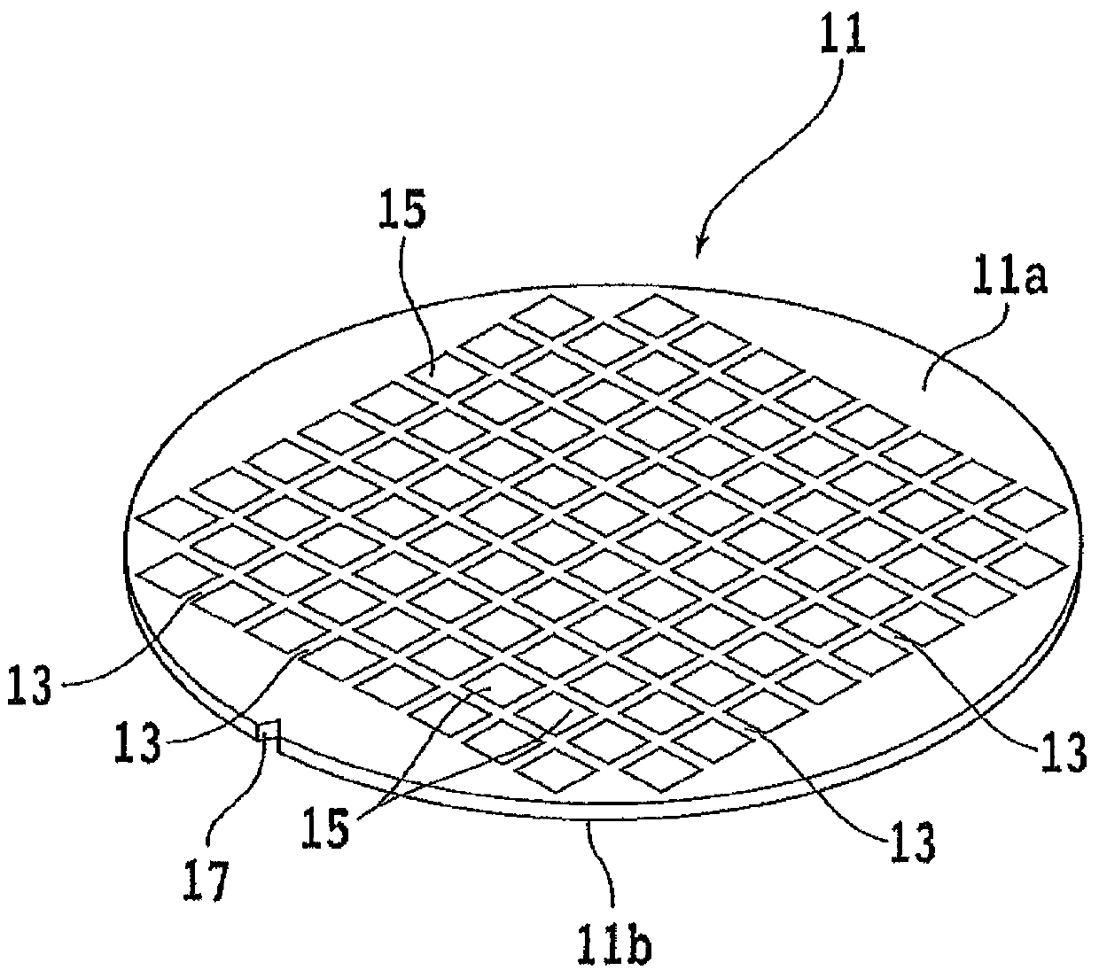
[0036] Hereinafter, embodiments of the present invention will be described in detail with reference to the drawings. refer to figure 1 , shows a front side perspective view of the semiconductor wafer 11 . Devices 15 such as ICs and LSIs are formed in regions divided by a plurality of dividing lines (streets) 13 on a front surface 11a of a semiconductor wafer (hereinafter sometimes simply referred to as a wafer) 11 . On the outer periphery of the wafer 11 is formed a notch 17 as a mark indicating the crystal orientation of the wafer.

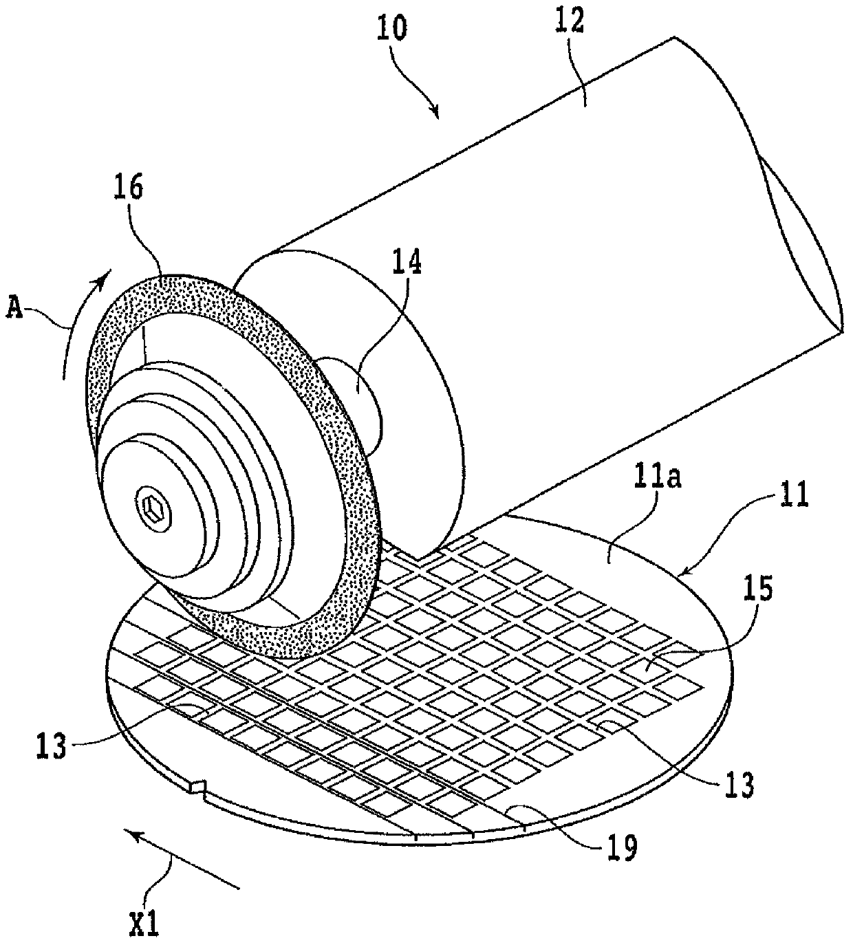
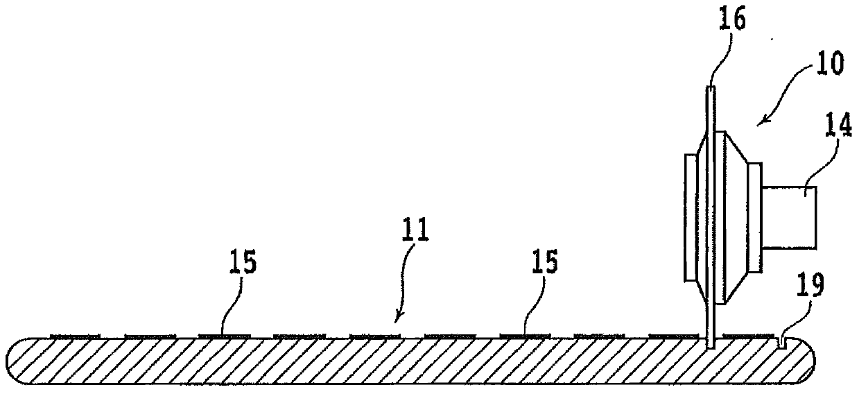
[0037] In the wafer processing method of the present invention, first, a groove forming step is performed in which a plurality of grooves are formed from the front surface 11a of the wafer 11 along the planned dividing line 13 to a depth not reaching the finished thickness. figure 2 is a perspective view showing a groove forming step, image 3 is its cross-sectional view. exist figure 2 and image 3 In , the chuck table for holding the wa...


PUM


Abstract

The invention provides a wafer processing method. The bending strength of a chip is not reduced, and a thick chip can be formed. A wafer is provided with a plurality of crossed predetermined cutting lines. The wafer processing method is characterized by comprising a groove forming step, a protective belt pasting step, a laser processing step and a grinding step. In the groove forming step, a plurality of grooves at certain depths are formed in the front side of the wafer along the predetermined cutting lines, and the wafer does not reach the final thickness. In the protective belt pasting step, a protective belt is pasted on the front side of the wafer. In the laser processing step, the focus of a laser beam which has a certain length and can penetrate the wafer is positioned on the position, in the wafer, being closer to the back side relative to the final thickness, the laser beam irradiates the back side of the wafer along the predetermined cutting lines, a deteriorative layer along the predetermined cutting line is formed in the wafer, and a crack layer which extends from the deteriorative layer to grooves and along the predetermined cutting lines. In the grinding step, a grinding member is employed to grind the back side of the wafer, and the wafer becomes thinner and reaches the final thickness, furthermore, the deteriorative layer is removed, and the wafer is cut along the predetermined cutting lines to form chips.

Description

technical field [0001] The present invention relates to a method for processing wafers such as semiconductor wafers. Background technique [0002] In the manufacturing process of semiconductor devices, ICs (Integrated Circuit: integrated circuits) are formed on the front surface of a roughly disc-shaped semiconductor wafer in a plurality of regions divided by planned division lines (separation lanes) formed in a grid pattern. , LSI (large scale integration: Large Scale Integration) and other devices, and each region in which the device is formed is divided along the planned dividing line, thereby manufacturing a device chip. [0003] As a dividing device for dividing a semiconductor wafer into individual device chips, a cutting device called a dicing device is generally used, which cuts the semiconductor wafer along the planned dividing line with a cutting blade having a very thin cutting edge, Divide a semiconductor wafer into individual device chips. The device chips thu...

Claims


Application Information

Patent Timeline
Patent Type & Authority Patents(China)
IPC IPC(8): H01L21/78B28D5/00
CPCB28D5/00B28D5/0005B28D5/0011H01L21/78H01L21/268H01L21/6836H01L21/76
Inventor 广泽俊一郎
Owner DISCO CORP
Why Eureka
Try Eureka