Check patentability & draft patents in minutes with Patsnap Eureka AI!

Array substrate, drive method of array substrate, display panel and display device

A technology of array substrate and substrate substrate, which is applied in static indicators, nonlinear optics, optics, etc., can solve the problem of high power consumption of data drive circuits, and achieve the effect of reducing power consumption

Inactive Publication Date: 2015-07-22
HEFEI XINSHENG OPTOELECTRONICS TECH CO LTD +1
View PDF6 Cites 5 Cited by
  • Summary
  • Abstract
  • Description
  • Claims
  • Application Information

AI Technical Summary

Problems solved by technology

Since the grayscale signal loaded by the data driving circuit to the data line will be loaded on the entire data line, coupling capacitance will be formed between the entire data line and each gate line and between the entire data line and the liquid crystal layer, resulting in The gray-scale signal loaded on the data line charges the pixel electrode and also charges the coupling capacitor corresponding to the entire data line, which in turn will cause a large power consumption of the data driving circuit

Method used


Image

  • Array substrate, drive method of array substrate, display panel and display device
  • Array substrate, drive method of array substrate, display panel and display device
  • Array substrate, drive method of array substrate, display panel and display device

Examples


Embodiment Construction

[0040] Specific implementations of an array substrate, a driving method thereof, a display panel, and a display device provided by the embodiments of the present invention will be described in detail below with reference to the accompanying drawings.

[0041] The shapes and sizes of the components in the drawings do not reflect the real scale of the array substrate, but are only intended to schematically illustrate the content of the present invention.

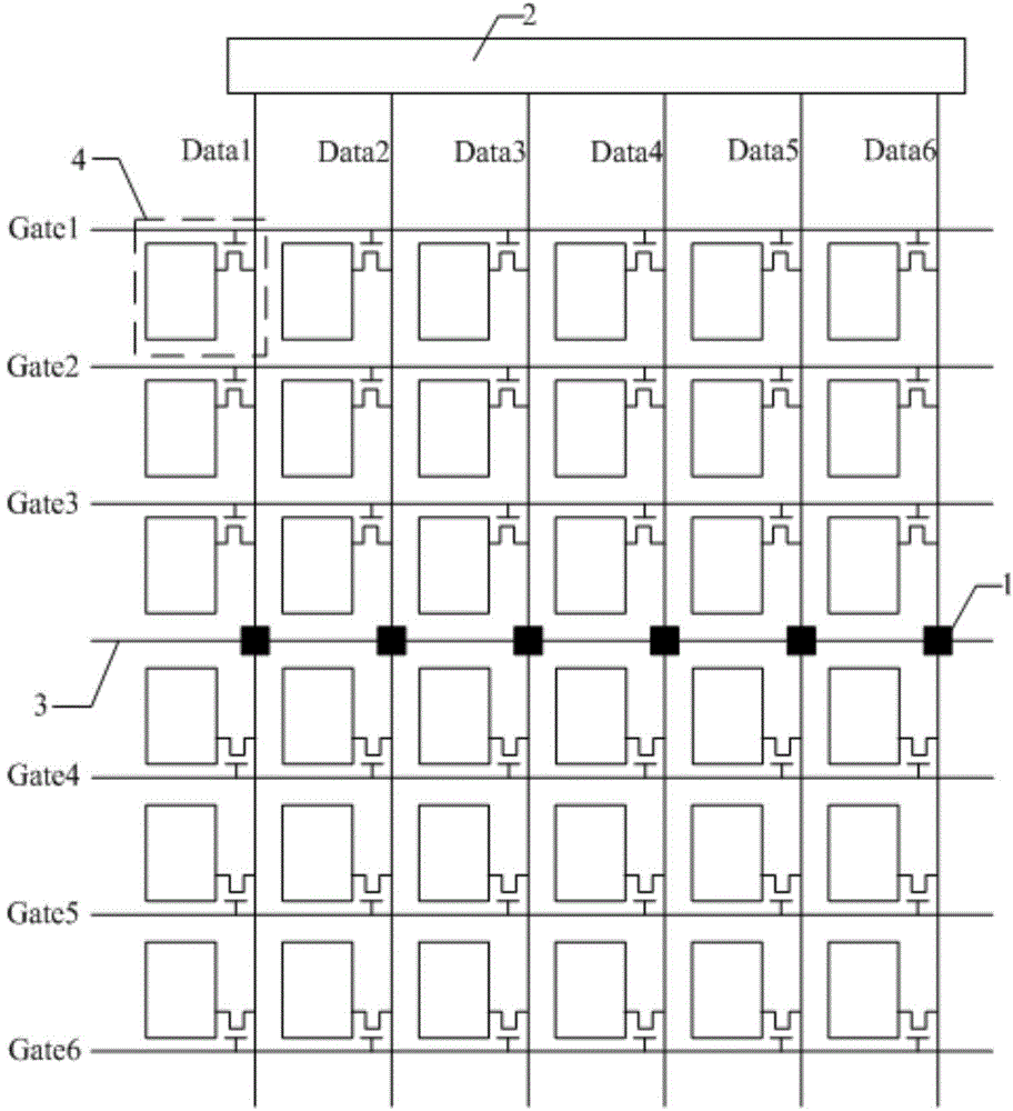
[0042] An array substrate provided by an embodiment of the present invention, such as figure 1 As shown, it includes: a base substrate and a plurality of gate lines Gate1, Gate2...Gate6 and a plurality of data lines Data1, Data2...Data6 ( figure 1 Take 6 gate lines and 6 data lines as an example for illustration); also include:

[0043] At least one switch 1 on at least one data line ( figure 1 Each data line is provided with a switch 1 as an example for illustration); each switch 1 is used to conduct or disconnect the two p...


PUM


Abstract

The invention discloses an array substrate, a drive method of the array substrate, a display panel and a display device. In the array substrate, at least one data line is provided with at least one switch, each switch is used for connecting or disconnecting of two parts of data lines electrically connected with the switch, and a control component is used for controlling connection or disconnection of each switch according to the position relation of a data drive circuit, a current scanned grid line and each switch. When a grid electrode scanning signal is loaded on the grid line located between each switch and the data drive circuit, the control component can control the switch to be disconnected. When a grid line scanning signal is loaded on the grid line on the side, back away from the data drive circuit, of each switch, the control component can control the switch to be connected. Accordingly, a gray scale signal loaded by the data drive circuit to the data line does not need to be loaded to the whole data line, and when a pixel electrode is charged through the gray scale signal, coupling capacitors corresponding to part of data lines are charged, and therefore the power consumption of the data drive circuit can be reduced.

Description

technical field [0001] The present invention relates to the field of display technology, in particular to an array substrate, a driving method thereof, a display panel and a display device. Background technique [0002] With the continuous development of display technology, light emitting diode (Light Emitting Diode, LED), organic light emitting diode (Organic Light Emitting Diode, OLED), plasma display (Plasma Display Panel, PDP) and liquid crystal display (Liquid Crystal Display, LCD) etc. Flat panel displays are developing rapidly. [0003] The existing liquid crystal display is taken as an example for description. Existing liquid crystal displays include an array substrate, an opposite substrate, and a liquid crystal layer located between the two substrates; wherein, gate lines, data lines, thin film transistors (Thin Film Transistor, TFT) and pixel electrodes are generally arranged on one side of the array substrate. . When the gate drive circuit inputs a high-potent...

Claims


Application Information

Patent Timeline
IPC IPC(8): G02F1/133G02F1/1362G09G3/36
CPCG02F1/13306G02F1/1362G02F1/136227G02F1/13624G02F1/136286G09G3/3611G09G2320/0223G09G3/3688G09G3/3677G09G2330/021
Inventor 刘荣铖
Owner HEFEI XINSHENG OPTOELECTRONICS TECH CO LTD
Features
  • R&D
  • Intellectual Property
  • Life Sciences
  • Materials
  • Tech Scout
  • Unparalleled Data Quality
  • Higher Quality Content
  • 60% Fewer Hallucinations
Learn More