Layout method and device for realizing interference-free power supply of internal analog modules of chip

An analog module, non-interference technology, applied in the direction of electrical digital data processing, special data processing applications, instruments, etc., can solve the problems of increasing the number of chip metal layers, wasting chip resources, increasing costs, etc., to improve accuracy, reduce costs, Avoid the effects of noise coupling

Active Publication Date: 2018-01-05
CAPITAL MICROELECTRONICS
View PDF4 Cites 0 Cited by
  • Summary
  • Abstract
  • Description
  • Claims
  • Application Information

AI Technical Summary

Problems solved by technology

[0002] There are multiple analog modules inside the system-level chip. The general power supply planning scheme adopts a point-to-point method. The chip power supply will be distributed to various positions inside the chip, which wastes chip resources, increases costs, and increases the number of metal layers of the chip.

Method used


Image

  • Layout method and device for realizing interference-free power supply of internal analog modules of chip
  • Layout method and device for realizing interference-free power supply of internal analog modules of chip
  • Layout method and device for realizing interference-free power supply of internal analog modules of chip

Examples


Embodiment Construction

[0014] In order to enable those skilled in the art to better understand the technical solutions in the embodiments of the present invention, and to make the above-mentioned purposes, features and advantages of the embodiments of the present invention more obvious and understandable, the following describes the technical solutions of the present invention through the accompanying drawings and embodiments The technical solution is further described in detail. Based on the embodiments of the present invention, all other embodiments obtained by persons of ordinary skill in the art without creative efforts fall within the protection scope of the present invention.

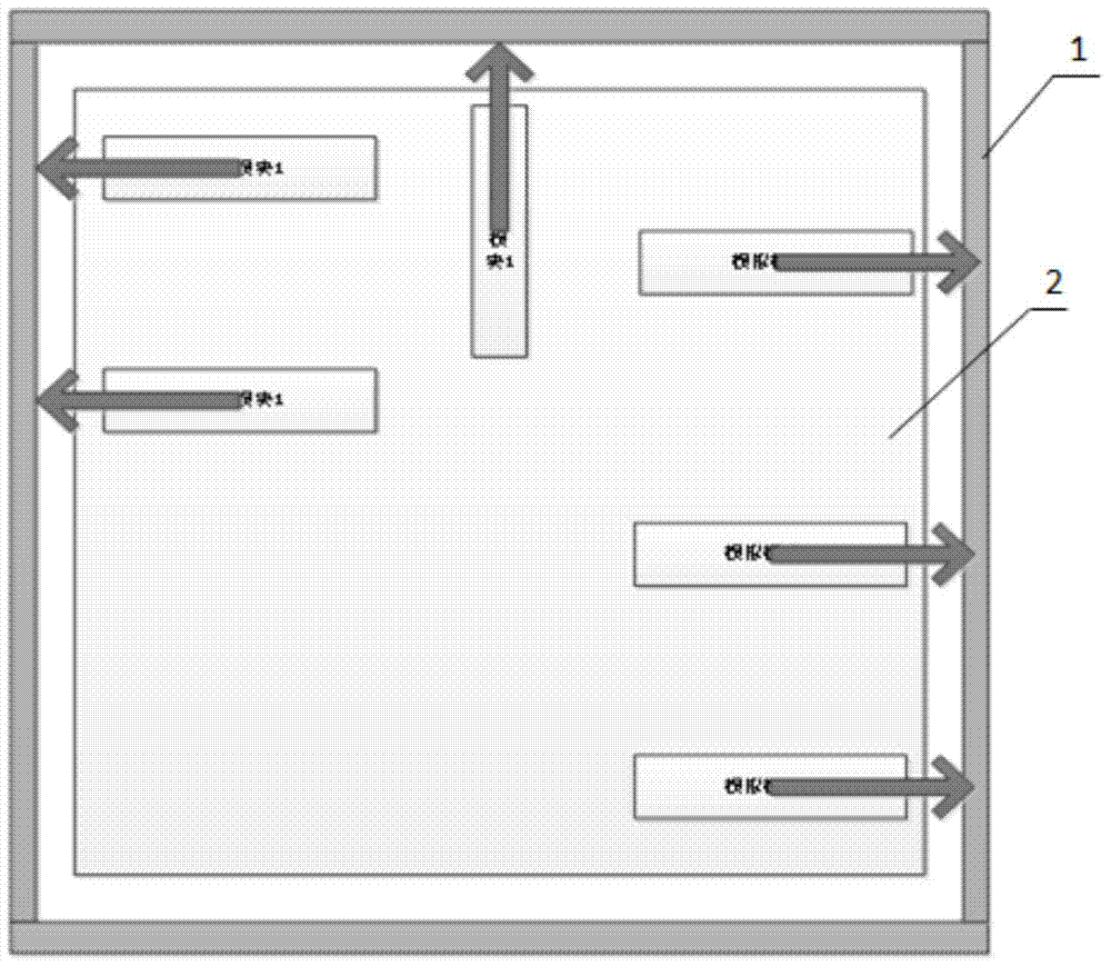
[0015] figure 1 It is a schematic plan view of the layout device to realize the interference-free power supply of the analog module inside the chip.

[0016] Such as figure 1 As shown, the device of the present invention includes a chip 1 and a power ring 2, the chip 1 includes N pieces, and the power ring 2 includes ...


PUM


Abstract

The invention provides a layout method and a device for realizing interference-free power supply of an analog module inside a chip. The device includes N chips and a power supply ring with N layers of metal rings, the first layer and the Nth layer are respectively a single metal ring, and the second layer to N-1 layer respectively include the first, second and third metal rings ring; the Nth layer of the power ring is grounded, and the first metal sub-ring and the third metal sub-ring in the first layer, the Nth layer, and the second layer to the N-1 layer are connected to the ground through through holes; the second layer to the The second metal sub-ring in the N-1 partial layer is separated from the ground layer metal ring and used as a signal line or a power line; the third metal sub-ring in a partial layer is disconnected at an appropriate position, and the signal line or power line passes through the disconnection and connects with the The analog modules inside the chip are connected. Through the invention, the length and width of the chip can be reduced by more than 30um. Effectively reduce costs and improve the accuracy of analog modules.

Description

technical field [0001] The invention relates to the technical field of semiconductor layout design, in particular to a layout method and a device for realizing interference-free power supply of an analog module inside a chip. Background technique [0002] There are multiple analog modules inside the system-level chip. The general power planning scheme adopts a point-to-point method. The chip power supply will be distributed to various positions inside the chip, which wastes chip resources, increases costs, and increases the number of metal layers of the chip. The general analog power wiring method in the chip generally starts from the power pad, uses an independent power line to start from the edge of the chip as far as possible away from the noisy module, walks to the position of the analog module, and connects to the power supply of the analog module. The power line runs from the inside of the chip and passes through various digital modules, which will be coupled with the ...

Claims


Application Information

Patent Timeline
Patent Type & Authority Patents(China)
IPC IPC(8): G06F17/50
Inventor 刘成利陈子贤刘明
Owner CAPITAL MICROELECTRONICS
Why Eureka
Try Eureka