Supercharge Your Innovation With Domain-Expert AI Agents!

Silicon carbide power component

A technology of power components and silicon carbide, applied in the direction of electrical components, semiconductor devices, circuits, etc., can solve the problem of adding steps

Active Publication Date: 2015-07-22
SHANGHAI HESTIA POWER INC
View PDF5 Cites 2 Cited by
  • Summary
  • Abstract
  • Description
  • Claims
  • Application Information

AI Technical Summary

Problems solved by technology

[0004] However, the above-mentioned method is to additionally form the buffer layer to improve the ability of the power device to withstand the breakdown voltage, so that the power device not only needs to increase the steps of making the buffer layer in the process, but also the power device is resistant to the breakdown voltage There is still room for improvement

Method used


Image

  • Silicon carbide power component
  • Silicon carbide power component
  • Silicon carbide power component

Examples


Embodiment Construction

[0015] Relevant detailed description and technical content of the present invention, now just explain as follows with respect to matching drawing:

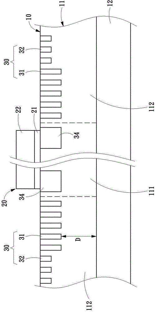
[0016] see figure 1 As shown, it is a schematic structural diagram of the first embodiment of the present invention, as shown in the figure: the present invention provides a silicon carbide power element with a terminal structure, including a silicon carbide substrate 10, a power element structure 20 and a terminal structure 30 . The silicon carbide substrate 10 includes a base layer 12 and a drift layer 11 on the base layer 12. Both the base layer 12 and the drift layer 11 have a first conductivity. In this embodiment, the first conductivity can be For N-type doping, the base layer 12 has an electron concentration greater than that of the drift layer 11, but not limited thereto. The drift layer 11 further includes an active region 111 and a termination region 112 , and the termination region 112 surrounds the active region 111 ...


PUM


Abstract

A silicon carbide power component comprises a silicon carbide substrate, a power component structure and a terminal structure. The silicon carbide substrate comprises a drift layer, and the drift layer with first conductivity comprises an active area and a terminal area. The power component structure is arranged in the active area. The terminal structure with second conductivity is arranged in the terminal area, and comprises at least one first doped ring and at least one second doped ring, wherein the first doped ring surrounds the power component structure and is adjacent to the power component structure, and the second doped ring surrounds the first doped ring. The first doped concentration of the first doped ring is lower than the doped concentration of the second doped ring, and the first doped depth of the first doped ring is greater than the doped depth of the second doped ring, and thus, the collapse voltage of the silicon carbide power component is improved.

Description

technical field [0001] The invention relates to a semiconductor element, especially a power element with a terminal structure. Background technique [0002] Power components can be widely used to form various switching components, such as switches of power supplies, telecommunication switches, power switches, etc., which require not only the ability to pass large currents in the active area, but also the ability to withstand large loads in the terminal area. breakdown voltage. [0003] Therefore, for power components, in addition to the active area that can conduct current in the design, it is also necessary to design a terminal structure that can avoid early collapse during reverse bias operation, so as to improve the reliability of the component. The types of traditional terminal structures are: local oxidation of silicon (LOCOS), electric field plate (field plate), and guard ring (guard ring), etc., and in US Patent Publication No. US20100032685, a power element with a t...

Claims


Application Information

Patent Timeline
IPC IPC(8): H01L29/06H01L29/78H01L29/872
CPCH01L29/0619H01L29/24H01L29/78H01L29/872
Inventor 李传英李隆盛颜诚廷洪建中
Owner SHANGHAI HESTIA POWER INC
Features
  • R&D
  • Intellectual Property
  • Life Sciences
  • Materials
  • Tech Scout
  • Unparalleled Data Quality
  • Higher Quality Content
  • 60% Fewer Hallucinations
Learn More