TFT (thin film transistor) array substrate

An array substrate and pixel technology, applied in instruments, semiconductor devices, optics, etc., can solve the problems of aggravated resistance-capacitance delay, crowded fan-out area, and increased cost of driver ICs, so as to improve color shift, reduce costs, and ensure charging efficiency effect

Active Publication Date: 2015-07-29
TCL CHINA STAR OPTOELECTRONICS TECH CO LTD
View PDF5 Cites 32 Cited by
  • Summary
  • Abstract
  • Description
  • Claims
  • Application Information

AI Technical Summary

Problems solved by technology

[0006] Although the above-mentioned existing TFT array substrate using 2D1G technology can improve the color shift, this design needs to double the number of data lines, which not only increases the cost of the driver IC, but also causes congestion in the Fanout area. Increase resistance-capacitance delay (RC), reduce charging efficiency, and affect product competitiveness

Method used


Image

  • TFT (thin film transistor) array substrate
  • TFT (thin film transistor) array substrate
  • TFT (thin film transistor) array substrate

Examples


no. 1 example

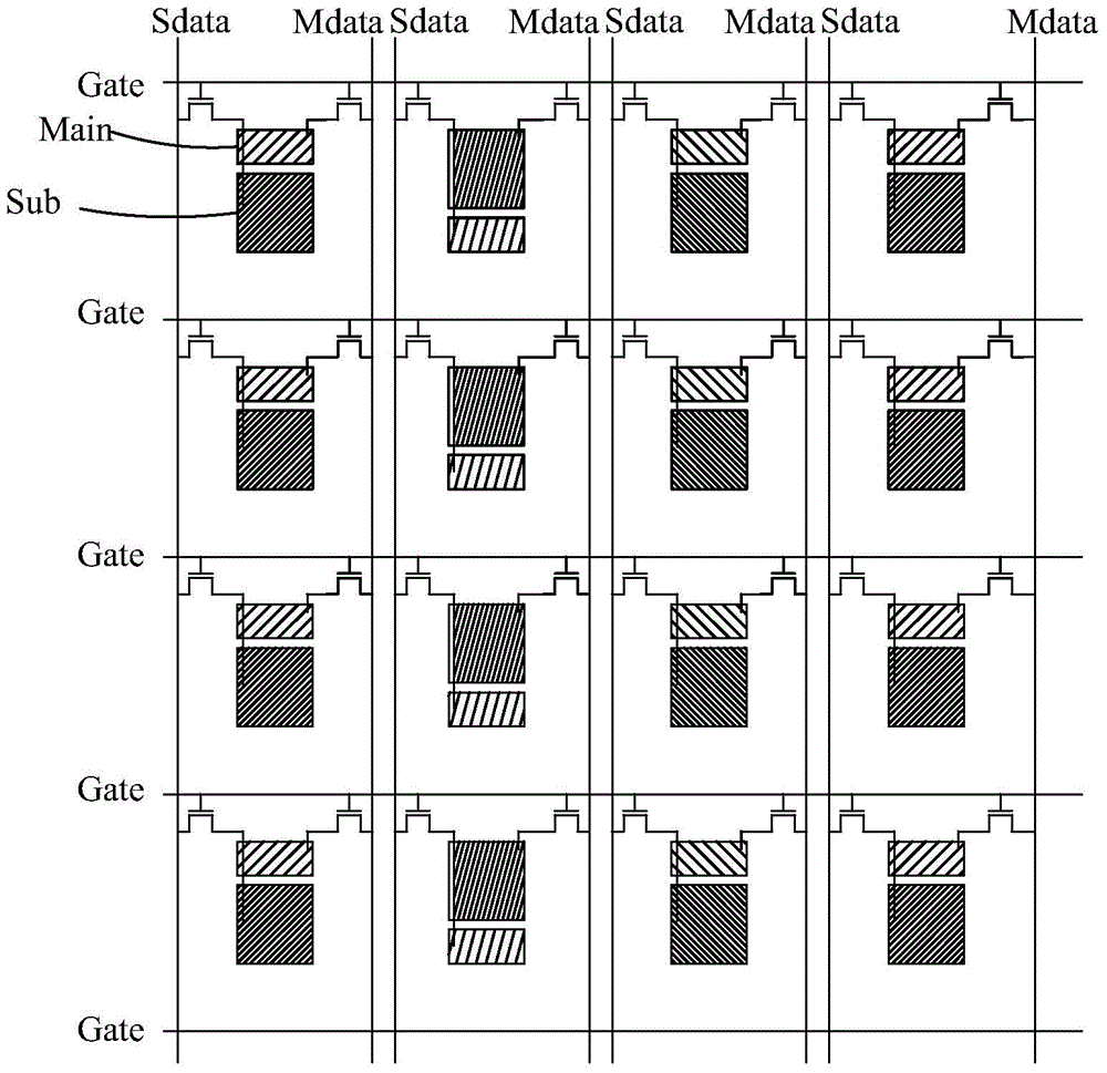
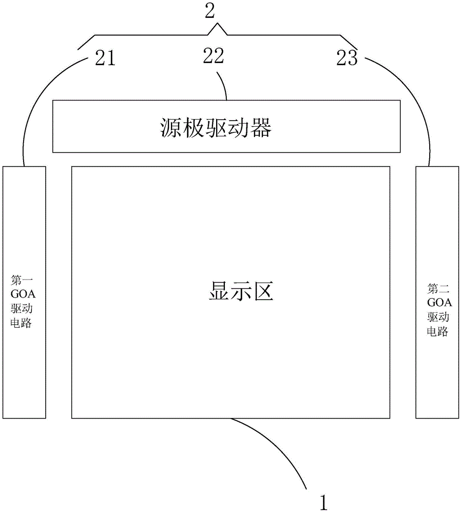
[0039] The invention provides a TFT array substrate. see image 3 , and combined with Figure 4 , which is the first embodiment of the present invention, the TFT array substrate includes: a display area 1 and a non-display area 2 arranged around the display area 1 .

[0040] The display area 1 is provided with: a plurality of vertical data lines parallel to each other and arranged in sequence, a plurality of horizontal scanning lines parallel to each other and arranged in sequence, and a plurality of sub-pixels arranged in an array.

[0041]Each sub-pixel is divided into a main area (indicated by a rectangle with a smaller area) and a sub-area (indicated by a rectangle with a larger area); the main area of ​​each sub-pixel is connected to a main area TFT TM, and each sub-pixel The secondary area is connected to the primary area TFT TS. exist Figure 4 In the shown first embodiment, in the same row of sub-pixels, the sub-pixels in every two adjacent columns are arranged in ...


PUM


Abstract

The invention provides a TFT (thin film transistor) array substrate. Compared with conventional TFT array substrates adopting the 2D1G technique, the TFT array substrate increases the number of scanning lines, so that the number of data lines is decreased by half, the data lines are divided into main data lines (MD) and sub data lines (SD), main areas of sub-pixels located at both sides of the main data lines (MD) are controlled by the main data lines (MD), sub-areas of the sub-pixels located at both sides of the sub data lines (SD) are controlled by the sub data lines (SD), and two GOA (Gate Driver on Array) drive circuits are respectively arranged at the left side and right side of a display area to bilaterally drive all the scanning lines. The TFT array substrate not only can improve the colour shift problem of VA (Vertical Alignment) type liquid crystal display panels, but also can ensure charging efficiency and reduce the cost of liquid crystal panels.

Description

technical field [0001] The present invention relates to the field of display technology, in particular to a TFT array substrate. Background technique [0002] A Liquid Crystal Display (LCD) has many advantages such as a thin body, power saving, and no radiation, and has been widely used. Such as: LCD TV, mobile phone, personal digital assistant (PDA), digital camera, computer screen or notebook computer screen, etc., occupy a dominant position in the field of flat panel display. [0003] Generally, a liquid crystal display panel is composed of a color filter substrate (Color Filter, CF), a thin film transistor array substrate (Thin Film Transistor Array Substrate, TFT Array Substrate), and a liquid crystal layer (Liquid Crystal Layer) disposed between the two substrates. Composition, and set pixel electrodes and common electrodes on the opposite inner sides of the two substrates, and control the liquid crystal molecules to change direction by applying a voltage, and refract...

Claims


Application Information

Patent Timeline
Patent Type & Authority Applications(China)
IPC IPC(8): G02F1/1362G02F1/1368G02F1/13
CPCG02F1/13624G02F1/136286G09G3/3611G09G3/3648G09G2300/0426G09G2300/0447G02F1/134345G02F1/1368G02F1/134336G09G3/3677G09G3/3688G09G2300/0452G09G2310/0251G09G2320/0242G09G2320/0247H01L27/124
Inventor 曹尚操
Owner TCL CHINA STAR OPTOELECTRONICS TECH CO LTD
Why Eureka
Try Eureka