Display apparatus

A display device and non-display technology, which is applied in the directions of identification devices, instruments, semiconductor devices, etc., can solve the problems of abnormal operation of the circuit part and easy changes in electrical characteristics, and achieve the effect of not easy to operate badly.

Active Publication Date: 2015-08-05
SHARP KK
View PDF7 Cites 4 Cited by
  • Summary
  • Abstract
  • Description
  • Claims
  • Application Information

AI Technical Summary

Problems solved by technology

On the other hand, oxide semiconductors tend to change their electrical characteristics when moisture enters them, which causes the above-mentioned problem of abnormal operation of the circuit part.

Method used


Image

  • Display apparatus
  • Display apparatus
  • Display apparatus

Examples


Embodiment approach 1

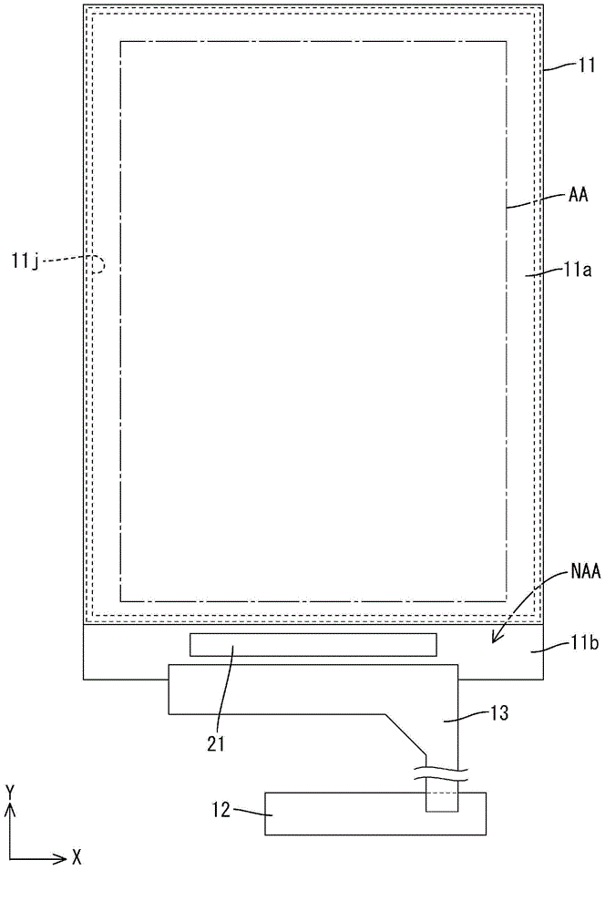
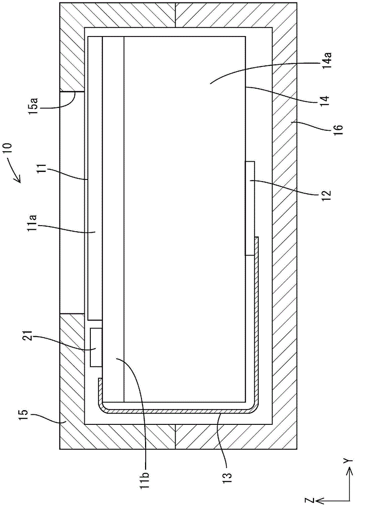
[0047] according to Figure 1 to Figure 14 Embodiment 1 of the present invention will be described. In this embodiment, a liquid crystal display device 10 is illustrated. In addition, X-axis, Y-axis, and Z-axis are shown in a part of each drawing, and it draws so that each axis direction may become the direction shown in each drawing. In addition, regarding the up-down direction, to Figure 2 to Figure 4 etc., and the upper side of the figure is the front side, and the lower side of the figure is the back side.

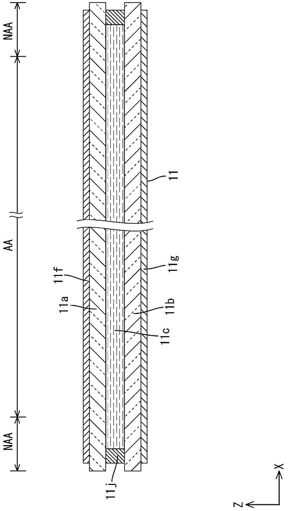
[0048] Such as figure 1 and figure 2 As shown, the liquid crystal display device 10 includes: a liquid crystal panel (display device, display panel) 1, which has a display portion AA capable of displaying images and disposed on the central side, and a non-display portion disposed on the outer peripheral side so as to surround the display portion AA. NAA; a driver (panel driver) 21 for driving the liquid crystal panel 11; a control circuit board (external signal ...

Embodiment approach 2

[0100] according to Figure 15 or Figure 16 Embodiment 2 of the present invention will be described. In this Embodiment 2, the structure which arrange|positions the common electrode part 122 on the side of the CF substrate 111a is shown. Note that redundant descriptions of the same configurations, actions, and effects as those of the first embodiment described above will be omitted.

[0101] Such as Figure 15 As shown, the common electrode portion 122 of the liquid crystal panel 111 in this embodiment is not arranged on the side of the array substrate 111b having the TFT 117 for the display unit, but on the side of the CF substrate 111a, and the operation mode is VA (Vertical Alignment: vertical alignment) model. The common electrode portion 122 is arranged to be interposed between the alignment film 111d, the color filter 111h, and the light-shielding layer 111i, and is a solid pattern covering almost the entire surface of the CF substrate 111a. On the array substrate ...

Embodiment approach 3

[0103] according to Figure 17 to Figure 19 Embodiment 3 of the present invention will be described. In this Embodiment 3, the structure which arrange|positioned the plane of each gate electrode part 217a, 229a of each TFT217,229 is shown. Note that redundant descriptions of the same configurations, actions, and effects as those of the first embodiment described above will be omitted.

[0104] Such as Figure 17 and Figure 18 As shown, the first gate electrode portion 217 a constituting the TFT 217 for a display portion is formed integrally without branching from the gate wiring 219 . That is, the TFT 217 for a display portion is disposed so as to be placed entirely on the gate wiring 219 . Therefore, the first channel portion 217d constituting the TFT 217 for a display portion is arranged to overlap with the first gate electrode portion 217a (gate wiring 219 ) over the entire area in plan view. same, Figure 17 and Figure 19 As shown, the second gate electrode portio...


PUM

PropertyMeasurementUnit
thicknessaaaaaaaaaa
thicknessaaaaaaaaaa
thicknessaaaaaaaaaa

Abstract

A liquid crystal panel (11) is provided with: a display section TFT (17), which is disposed on a display section (AA) of an array substrate (11b); a non-display section TFT (29), which is disposed on a non-display section (NAA); a second gate electrode section (29a) constituting the non-display section TFT (29); a second channel section (29d) formed of an oxide semiconductor film (36); a second source electrode section (29b) connected to the second channel section (29d); a second drain electrode section (29c) connected to the second channel section (29d); and a first interlayer insulating film (39), which is laminated at least on the second source electrode section (29b) and the second drain electrode section (29c). The first interlayer insulating film (39) has a laminated structure having laminated therein: a lower layer-side first interlayer insulating film (39a), which is disposed relatively on the lower layer side, and which contains at least silicon and oxygen; and an upper layer-side first interlayer insulating film (39b), which is disposed relatively on the upper layer side, and which contains at least silicon and nitrogen, said upper layer-side first interlayer insulating film (39b) having a film thickness within the range of 35-75 nm.

Description

technical field [0001] The present invention relates to display devices. Background technique [0002] In a liquid crystal panel used in a liquid crystal display device, a plurality of TFTs are provided in a matrix as switching elements for controlling the operation of each pixel. Conventionally, a silicon semiconductor such as amorphous silicon is generally used as a semiconductor film used in a TFT, but in recent years a technique of using an oxide semiconductor with higher electron mobility as a semiconductor film has been proposed. An example of a liquid crystal display device using such a TFT using an oxide semiconductor as a switching element is described in Patent Document 1 below. [0003] prior art literature [0004] patent documents [0005] Patent Document 1: Japanese Unexamined Patent Publication No. 2011-29373 [0006] (problem to be solved by the invention) [0007] Due to the high electron mobility of oxide semiconductors, TFTs can be further miniaturize...

Claims


Application Information

Patent Timeline
Patent Type & Authority Applications(China)
IPC IPC(8): G09F9/30G02F1/1368H01L21/336H01L29/786
CPCH01L27/1222G02F1/136227H01L29/7869G02F1/1333G02F1/133345G02F1/1339G02F1/1343G02F1/13439G02F1/1362G02F1/1368H01L29/786H01L29/78606H01L27/1225G02F1/136286H01L27/124H01L29/24H01L29/45
Inventor 高西雄大原义仁中田幸伸
Owner SHARP KK
Why Eureka
Try Eureka