Semiconductor device having vertical MOSFET of super junction structure, and method for production of same

A manufacturing method, semiconductor technology, applied in semiconductor/solid-state device manufacturing, semiconductor devices, semiconductor/solid-state device components, etc., can solve problems such as PN column depth deviation, film thickness grinding stop, and manufacturing cost increase

Inactive Publication Date: 2015-08-12
DENSO CORP
View PDF6 Cites 1 Cited by
  • Summary
  • Abstract
  • Description
  • Claims
  • Application Information

AI Technical Summary

Problems solved by technology

[0005] However, when making p - p - Type layer J5 and n - The flattening and polishing of the surface of the pattern layer J2 has a large variation, and the depth of the PN column varies, and the desired depth cannot be obtained with high precision.
The reason is that, although there is also the problem of the precision of the epitaxial growth itself, to a greater extent, p - Type layer J5 and n - The planarization polishing of the type layer J2 becomes the polishing process of the same semiconductor material (such as silicon), and it is difficult to stop polishing at the desired film thickness in principle.
In addition, when the depth of the PN column varies in this way, the withstand voltage of the semiconductor device varies and the device characteristics deteriorate.
[0006] In addition, there is also the problem of using p on the SJ structure after forming the SJ structure - Type layer J6 grows epitaxially, but due to the surface of the SJ structure and the p - The inter-constructive handling of type layer J6, while the upper side of the p - Abnormal growth of type layer J6 degrades device characteristics
[0007] Furthermore, since independently performing p - The formation process of the type layer J6, so there are also problems such as increased manufacturing steps and higher manufacturing costs.

Method used


Image

  • Semiconductor device having vertical MOSFET of super junction structure, and method for production of same
  • Semiconductor device having vertical MOSFET of super junction structure, and method for production of same
  • Semiconductor device having vertical MOSFET of super junction structure, and method for production of same

Examples


no. 1 approach

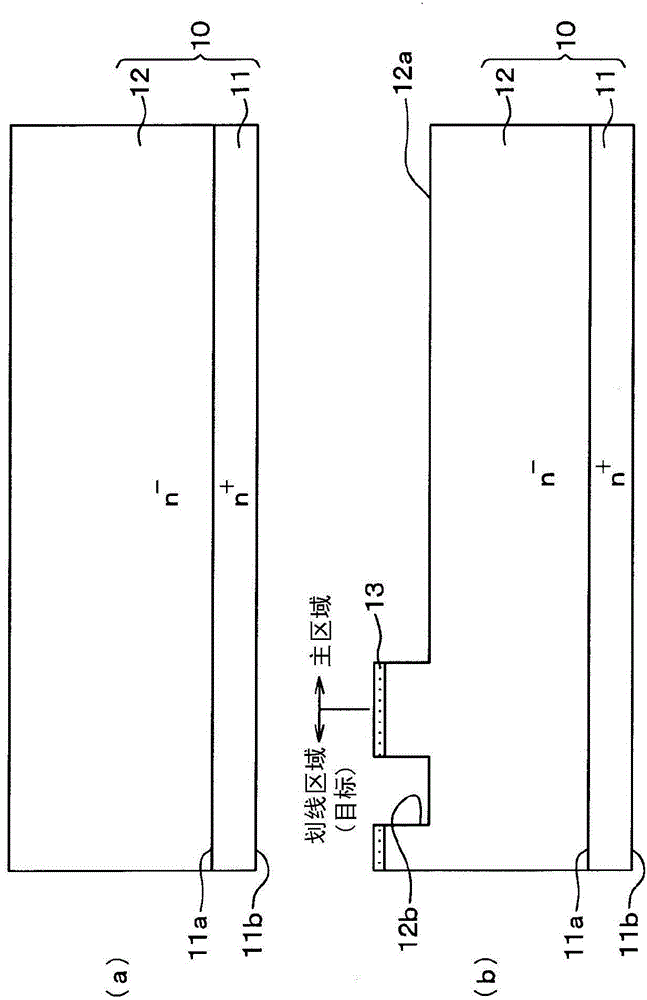
[0043] refer to figure 1 (a) to figure 2 (b) The method of manufacturing the semiconductor device according to the first embodiment of the present invention will be described. In addition, here, a semiconductor device including a trench-gate vertical MOSFET as an SJ-structure vertical MOSFET will be described as an example.

[0044] 〔 figure 1 Process shown in (a)]

[0045] The following semiconductor substrate 10 is prepared: n + On the surface 11a of the type silicon substrate 11, the n corresponding to the first semiconductor layer - Type layer 12 is grown epitaxially. no + Type silicon substrate 11 is the part that functions as the drain region, and n - The n-type layer 12 has a higher concentration of impurities than the n-type. no - Type layer 12 functions as a drift layer and constitutes an n-type column among PN columns.

[0046] 〔 figure 1 Process shown in (b)]

[0047] On the surface side of the semiconductor substrate 10, at n -The oxide film 13 is ...
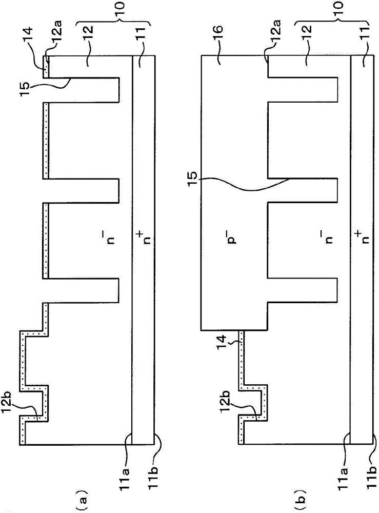
no. 2 approach

[0067] A second embodiment of the present invention will be described. In the present embodiment, the vertical MOSFET formed in the semiconductor device is changed to a planar type compared to the first embodiment, and the rest is the same as the first embodiment, so only the parts different from the first embodiment will be described.

[0068] refer to Figure 4 (a) and Figure 4 (b) A method of manufacturing the vertical MOSFET of the present embodiment will be described.

[0069] First, after performing the description in the first embodiment figure 1 (a), figure 1 (b), figure 2 (a), figure 2 After the process of (b), as Figure 4 The process of (a) is carried out as described in the first embodiment. image 3 (a) The same process. Thus, a structure is formed in which, on the surface side of the semiconductor substrate 10 , including the concave portion 12 a and the groove 15 , the n- type layer 12 on the surface so that p - Type layer 16 epitaxial growth, and ...
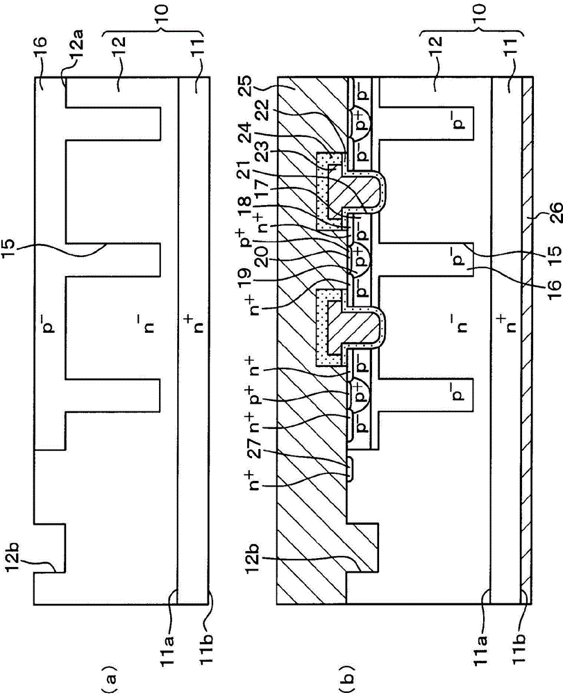
no. 3 approach

[0075] A third embodiment of the present invention will be described. The present embodiment is a manufacturing method in consideration of the peripheral withstand voltage structure of the semiconductor device compared to the second embodiment, and the rest is the same as the second embodiment, so only the differences from the second embodiment will be described.

[0076] refer to Figure 5 (a)~ Figure 7 (b) The vertical MOSFET manufacturing method of this embodiment, that is, the manufacturing method that further includes a step of forming a peripheral voltage-resistant structure in a semiconductor device including a planar vertical MOSFET having an SJ structure will be described.

[0077] First, in Figure 5 In the process shown in (a), prepare the n substrate as a substrate made of semiconductor material having a surface 11a and a back surface 11b. + On the surface 11a of the type silicon substrate 11, the n corresponding to the first semiconductor layer - The substrat...


PUM


Abstract

The present invention provides a semiconductor device having vertical MOSFET of super junction structure, and a method for production of same. The method for production of a semiconductor device has the steps of preparing a semiconductor substrate (10) in which a first semiconductor layer (12) formed on a substrate (11), forming a first recessed portion (12a) in the first semiconductor layer, forming a plurality of trenches (15) in the first semiconductor layer within the first recessed portion, epitaxially growing a second semiconductor layer (16) to fill in the trenches and the recessed portion, forming an SJ structure having a PN columns comprising the first semiconductor layer between the plurality of trenches and the second semiconductor layer within the trenches, forming over the SJ structure a channel layer (17) and a source region (18) contacting the channel layer, forming a gate electrode (23) on an intervening gate insulation film (22) over the channel layer, forming a source electrode (25); that connects to the source region, and forming a drain electrode (26) on the back surface of the substrate, to form a vertical MOSFET.

Description

[0001] This application is based on Japanese application No. 2012-268412 filed on December 7, 2012, Japanese application No. 2012-268413 filed on December 7, 2012, and Japanese application No. 2013-222256 filed on October 25, 2013 No., and the contents described in these applications are referred to in the present application. technical field [0002] The present invention relates to a semiconductor device having a vertical MOSFET having a superjunction (hereinafter referred to as SJ) structure formed by epitaxially growing a second semiconductor layer in a trench formed in a first semiconductor layer, and a method for manufacturing the same. SJ construction. Background technique [0003] Conventionally, there is known a semiconductor device having an SJ structure in which n-type columns and p-type columns are alternately and repeatedly formed (for example, refer to Patent Document 1). When manufacturing a semiconductor device with an SJ structure, for example Figure 9 As ...

Claims


Application Information

Patent Timeline
Patent Type & Authority Applications(China)
IPC IPC(8): H01L29/78H01L21/336
CPCH01L29/7813H01L23/544H01L29/0615H01L29/0634H01L29/1095H01L29/66734H01L29/7811H01L2223/54426H01L2223/5446H01L2924/0002
Inventor 江口浩次小田洋平
Owner DENSO CORP
Why Eureka
Try Eureka