

Method for representing amorphous alloy microstructure
A technology of microstructure and characterization, which is applied in the field of microstructure characterization and characterization of the microstructure of amorphous alloys, can solve the problems of lack of effective technical methods and the inability to characterize the three-dimensional structural characteristics of amorphous alloy atomic clusters, etc., and achieve reliable technology and excellent softness. Magnetic properties and mechanical properties, repeatable effect
- Summary
- Abstract
- Description
- Claims
- Application Information
AI Technical Summary
Problems solved by technology
Method used
Image

Examples
preparation example Construction
[0034] In the preparation step of the sample, the amorphous material is successively subjected to wire cutting, acetone ultrasonic treatment, ultrasonic cutting into discs, bonding sample holder, heat curing, flat grinding, pitting (ie mechanical thinning), ion beam Thinning, and finally the desired sample is prepared.
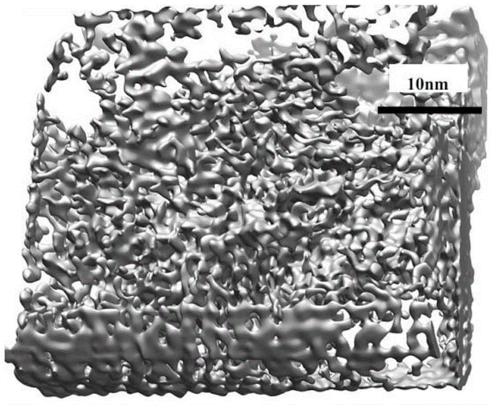
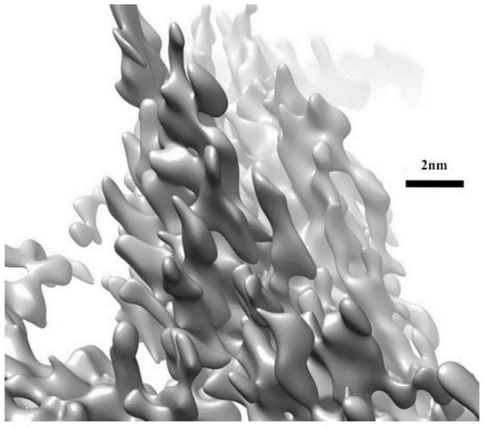
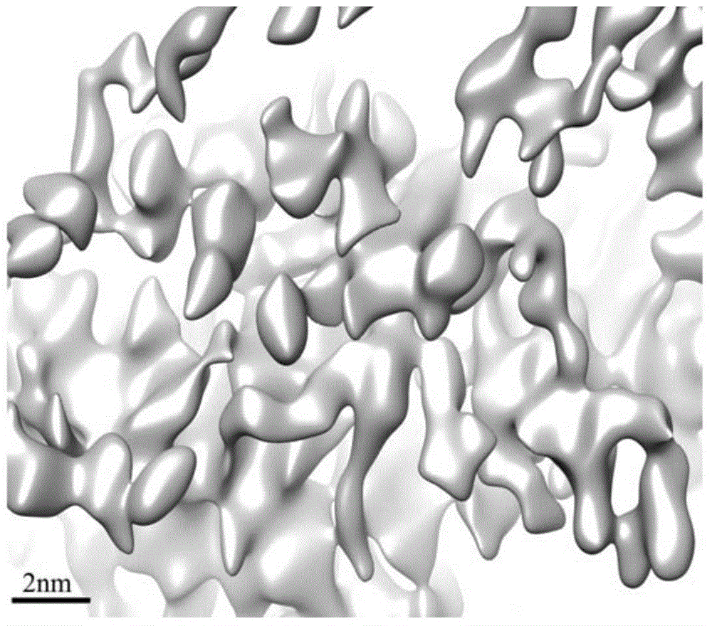
[0035] The thickness of the sample is 0.5-500nm (such as 0.6nm, 5nm, 10nm, 50nm, 70nm, 100nm, 150nm, 200nm, 260nm, 300nm, 350nm, 400nm, 450nm, 490nm), preferably, the thickness of the sample The size is 6-100 nm (such as 7 nm, 10 nm, 15 nm, 25 nm, 40 nm, 50 nm, 60 nm, 70 nm, 80 nm, 90 nm). The method of the present invention can characterize samples with a thickness exceeding 6 nm. The sample thickness range of the present invention is much wider than the current high-cost Angstrom-scale electron beam method, which usually requires samples below 5nm.
[0036] Preferably, the thickness of the sheet after wire cutting is not greater than 0.5mm (such as 0.1mm, ...
Embodiment 1
[0050] Using Zr 48 Cu 45 Al 7 (The subscript number is at%) amorphous alloy. The amorphous alloy is prepared by a common copper mold casting method in the field.
[0051] The method for characterizing the above amorphous alloys is as follows:
[0052] Step 1: including the following sub-steps in turn: (1) cutting the amorphous alloy material into thin slices with a thickness of 0.2 mm using a wire cutting machine (South Bay Technology inc. model: 650); (2) placing the thin slices in acetone for ultrasonication Treat for 20min; (3) Cut the thin slices after the ultrasonic treatment of acetone into discs with an ultrasonic cutting machine (Gatan model: 601), and the specifications are (4) Bond the wafer to the sample holder; (5) Place the wafer with the bracket in a heating furnace for heating and curing, the heating temperature is 70°C, and the heating time is 15 minutes; (6) The cured wafer is (7) Use a pit instrument (GATAN 656 type) to mechanically thin the polished waf...
Embodiment 2
[0057] Using Fe 80 Si 9 B 11 (the subscript number is at%) amorphous alloy, which is prepared by the rapid solidification method commonly used in this field.
[0058] Step 1: including the following sub-steps in turn: (1) cutting the amorphous alloy material into 0.3mm thin slices with a wire cutting machine (South Bay Technology inc. model: 650); (2) placing the thin slices in acetone for ultrasonication Treat for 20min; (3) Cut the thin slices after the ultrasonic treatment of acetone into discs with an ultrasonic cutting machine (Gatan model: 601), and the specifications are (4) Bond the wafer to the sample holder; (5) Place the wafer with the bracket in a heating furnace for heating and curing, the heating temperature is 70°C, and the heating time is 15 minutes; (6) The cured wafer is (7) Use a pit instrument (GATAN 656 type) to mechanically thin the polished wafer so that the center of the sample is as thin as 8 μm; (8) Use an ion thinner (GATAN model: 691) to The io...
PUM
| Property | Measurement | Unit |
|---|---|---|
| Thickness dimension | aaaaa | aaaaa |
| Thickness dimension | aaaaa | aaaaa |
| Thickness dimension | aaaaa | aaaaa |
Abstract
Description
Claims
Application Information