
Manufacturing method of vertical double-diffusion metal oxide semiconductor field effect transistor

An oxide semiconductor and vertical double-diffusion technology, which is applied in semiconductor/solid-state device manufacturing, electrical components, circuits, etc., can solve problems such as waste of manpower and material resources, changes in electrical parameters of VDMOS devices, and soft breakdown of VDMOS devices. To avoid waste and solve the effect of drain-source soft breakdown

Active Publication Date: 2015-08-26
FOUNDER MICROELECTRONICS INT
View PDF3 Cites 2 Cited by
  • Summary
  • Abstract
  • Description
  • Claims
  • Application Information

AI Technical Summary

Problems solved by technology

[0006] The invention provides a method for manufacturing a vertical double-diffused metal oxide semiconductor field effect transistor, which is used to solve the problem in the prior art that while solving the soft breakdown of the drain source of the VDMOS device, the remaining electrical parameters of the VDMOS device will be relatively large. Large changes, and the return of these electrical parameters to the target value wastes a lot of manpower and material resources

Method used


Image

  • Manufacturing method of vertical double-diffusion metal oxide semiconductor field effect transistor
  • Manufacturing method of vertical double-diffusion metal oxide semiconductor field effect transistor
  • Manufacturing method of vertical double-diffusion metal oxide semiconductor field effect transistor

Examples


Embodiment Construction

[0025] The technical solution of the present invention will be described in further detail below through specific embodiments and accompanying drawings.

[0026] figure 2 A schematic flowchart of an embodiment of a method for manufacturing a vertical double-diffused metal-oxide-semiconductor field effect transistor provided by the present invention. like figure 2 As shown, the method may specifically include:

[0027] S201, depositing an insulating layer on the surface of the silicon nitride layer.

[0028] S202, performing reflow treatment on the insulating layer at a set temperature, where the set temperature is lower than a threshold temperature of drain-source soft breakdown.

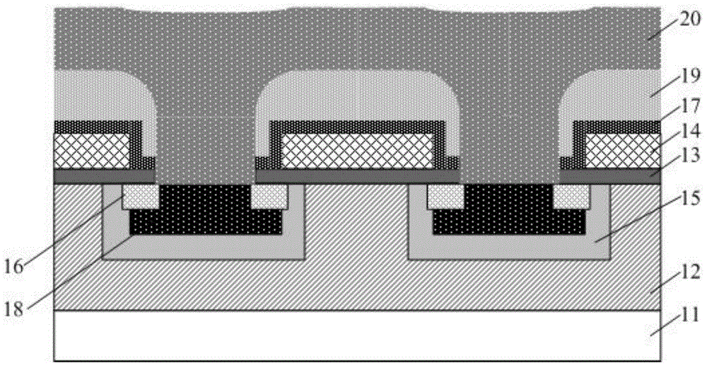
[0029] refer to figure 1 Those skilled in the art can understand that before step S201, the following steps are also included: sequentially forming an epitaxial layer 12, a gate oxide layer 13, a polysilicon layer 14, a body region 15, a source region 16, and a silicon nitride layer on the sub...


PUM


Abstract

The invention provides a manufacturing method of a vertical double-diffusion metal oxide semiconductor field effect transistor. The method comprises the steps of: depositing an insulating layer on the surface of a silicon nitride layer; and carrying out backflow processing on the insulating layer at a preset temperature, wherein the preset temperature is lower than a threshold temperature of drain source soft breakdown. According to the invention, the insulating layer is subjected to the backflow processing at the preset temperature lower than the threshold temperature of drain source soft breakdown. The temperature of the backflow processing is reduced, so that the transverse diffusion distance of a source region is shortened, the effective channel length of a body region is lengthened, the risk that a body region depletion layer breaks through to the source region under a junction reverse bias state of the device body region / epitaxial layer drift region is reduced, and the purpose of solving the drain source soft breakdown problem of a device is achieved. The method basically has no influences on other electric property parameter, and the wastes of manpower and material resources are avoided.

Description

technical field [0001] The invention relates to the technical field of manufacturing semiconductor devices, in particular to a method for manufacturing a vertical double-diffused metal oxide semiconductor field effect transistor. Background technique [0002] Vertical Double-diffusion Metal Oxide Semiconductor (VDMOS) combines the advantages of bipolar transistors and Metal Oxide Semiconductor (MOS) with nearly infinite Large quiescent input impedance and very fast switching times make it an ideal power device for both switching and linear applications. [0003] figure 1 It is a schematic diagram of the structure of a vertical double-diffused metal-oxide-semiconductor field effect transistor, such as figure 1 As shown, it includes: a substrate 11, an epitaxial layer 12 disposed on the surface of the substrate 11, a partially etched gate oxide layer 13 disposed on the surface of the epitaxial layer 12, and a partially etched gate oxide layer disposed on the surface of the g...

Claims


Application Information

Patent Timeline
IPC IPC(8): H01L21/336H01L21/3105
Inventor 刘竹张立荣
Owner FOUNDER MICROELECTRONICS INT
Learn More